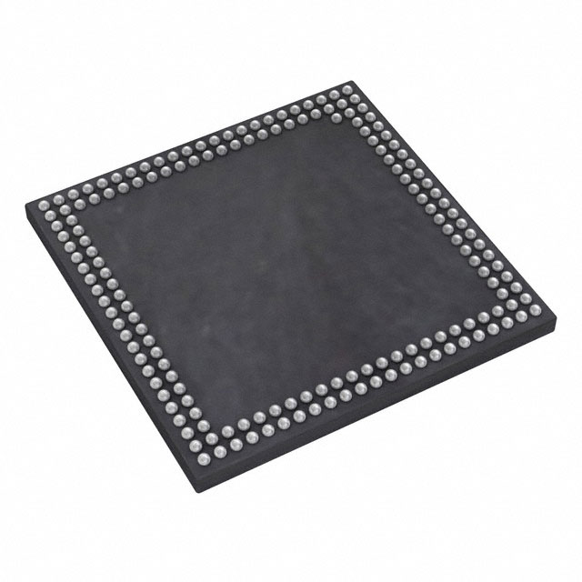
Embedded LPDDR2 SDRAM
Features
Embedded LPDDR2 SDRAM
EDB8132B4PB-8D-F
Features
Options
Marking
• Density/Chip select
– 8Gb/2-CS - dual die
• Organization
– x32
• VDD1/VDD2/VDDQ: 1.8V/1.2V/1.2V
• Revision
• FBGA “green” package
– 12mm x 12mm x 0.8mm, 168-ball
• Timing – cycle time
– 2.5ns @ RL = 6
• Operating temperature range
– From –30°C to +85°C
• Ultra-low-voltage core and I/O power supplies
• Frequency range
– 400 MHz (data rate: 800 Mb/s/pin)
• 4n prefetch DDR architecture
• 8 internal banks for concurrent operation
• Multiplexed, double data rate, command/address
inputs; commands entered on each CK_t/CK_c
edge
• Bidirectional/differential data strobe per byte of
data (DQS_t/DQS_c)
• Programmable READ and WRITE latencies (RL/WL)
• Burst length: 4, 8, and 16
• Per-bank refresh for concurrent operation
• Auto temperature-compensated self refresh
(ATCSR) by built-in temperature sensor
• Partial-array self refresh (PASR)
• Deep power-down mode (DPD)
• Selectable output drive strength (DS)
• Clock-stop capability
• Lead-free (RoHS-compliant) and halogen-free
packaging
81
32
B
4
PB
-8D
Blank
Table 1: Key Timing Parameters
Speed
Grade
Clock Rate
(MHz)
Data Rate
(Mb/s/pin)
RL
WL
8D
400
800
6
3
PDF: 09005aef85a1f01d
168b_2e0e_embedded_lpddr2_sdram.pdf – Rev. C 1/16 EN
1
Micron Technology, Inc. reserves the right to change products or specifications without notice.
© 2014 Micron Technology, Inc. All rights reserved.
Products and specifications discussed herein are subject to change by Micron without notice.
�Embedded LPDDR2 SDRAM
Features
Table 2: Configuration Addressing – Single-Channel Package
Architecture
256 Meg x 32
Density per package
8Gb
Die per package
2
Ranks per channel
1
Die per rank
2
Configuration
32 Meg x 16 x 8 banks x 2
Row addressing
16K A[13:0]
Column addressing
2K A[10:0]
Table 3: Part Number Description
Part
Number
EDB8132B4PB-8D-F-R,
EDB8132B4PB-8D-F-D
Total
Density
Configuration
Ranks
Channels
8Gb
256 Meg x 32
1
1
Package
Size
Ball
Pitch
12mm x 12mm
(0.80mm MAX height)
0.50mm
Figure 1: Marketing Part Number Chart
E
D
B
81 32
B
4
PB - 8D - F - D
Micron Technology
Packing Media
Type
D = Dry Pack (Tray)
R = Tape and Reel
D = Packaged device
Environment Code
F = Lead-free (RoHS-compliant)
and halogen-free
Product Family
B = Mobile LPDDR2 SDRAM
Density/Chip Select
Speed
81 = 8Gb/2-CS
8D = 800 Mb/s
Organization
Package
32 = x32
PB = BGA for PoP
Power Supply Interface
Revision
B = VDD1 = 1.8V, V DD2 = VDDQ = 1.2V,
S4B device, HSUL
Note:
1. The characters highlighted in gray indicate the physical part marking found on the device.
PDF: 09005aef85a1f01d
168b_2e0e_embedded_lpddr2_sdram.pdf – Rev. C 1/16 EN
2
Micron Technology, Inc. reserves the right to change products or specifications without notice.
© 2014 Micron Technology, Inc. All rights reserved.
�Embedded LPDDR2 SDRAM
Features
Contents
LPDDR2 Array Configuration ............................................................................................................................ 9
General Notes .............................................................................................................................................. 9
IDD Specifications – Dual Die, Single Channel .................................................................................................. 10
Package Block Diagrams ................................................................................................................................. 14
Package Dimensions ....................................................................................................................................... 15
Ball Assignments ............................................................................................................................................ 16
Ball Descriptions ............................................................................................................................................ 17
Functional Description ................................................................................................................................... 18
Simplified State Diagram ................................................................................................................................ 19
Power-Up and Initialization ............................................................................................................................ 21
Voltage Ramp and Device Initialization ....................................................................................................... 21
Initialization After RESET (Without Voltage Ramp) ...................................................................................... 23
Power-Off Sequence ....................................................................................................................................... 23
Uncontrolled Power-Off Sequence .............................................................................................................. 24
Mode Register Definition ................................................................................................................................ 24
Mode Register Assignments and Definitions ................................................................................................ 24
Commands and Timing .................................................................................................................................. 35
ACTIVATE Command ..................................................................................................................................... 36
8-Bank Device Operation ............................................................................................................................ 37
Read and Write Access Modes ......................................................................................................................... 38
Burst READ Command ................................................................................................................................... 38
READs Interrupted by a READ ..................................................................................................................... 45
Burst WRITE Command .................................................................................................................................. 45
WRITEs Interrupted by a WRITE ................................................................................................................. 48
BURST TERMINATE Command ...................................................................................................................... 48
Write Data Mask ............................................................................................................................................. 50
PRECHARGE Command ................................................................................................................................. 51
READ Burst Followed by PRECHARGE ......................................................................................................... 52
WRITE Burst Followed by PRECHARGE ....................................................................................................... 53
Auto Precharge operation ........................................................................................................................... 54
READ Burst with Auto Precharge ................................................................................................................. 54
WRITE Burst with Auto Precharge ............................................................................................................... 55
REFRESH Command ...................................................................................................................................... 57
REFRESH Requirements ............................................................................................................................. 59
SELF REFRESH Operation ............................................................................................................................... 66
Partial-Array Self Refresh – Bank Masking .................................................................................................... 68
Partial-Array Self Refresh – Segment Masking .............................................................................................. 68
MODE REGISTER READ ................................................................................................................................. 69
Temperature Sensor ................................................................................................................................... 71
DQ Calibration ........................................................................................................................................... 73
MODE REGISTER WRITE Command ............................................................................................................... 75
MRW RESET Command .............................................................................................................................. 75
MRW ZQ Calibration Commands ................................................................................................................ 76
ZQ External Resistor Value, Tolerance, and Capacitive Loading ..................................................................... 78
Power-Down .................................................................................................................................................. 78
Deep Power-Down ......................................................................................................................................... 85
Input Clock Frequency Changes and Stop Events ............................................................................................. 86
Input Clock Frequency Changes and Clock Stop with CKE LOW ................................................................... 86
Input Clock Frequency Changes and Clock Stop with CKE HIGH .................................................................. 87
NO OPERATION Command ............................................................................................................................ 87
PDF: 09005aef85a1f01d
168b_2e0e_embedded_lpddr2_sdram.pdf – Rev. C 1/16 EN
3
Micron Technology, Inc. reserves the right to change products or specifications without notice.
© 2014 Micron Technology, Inc. All rights reserved.
�Embedded LPDDR2 SDRAM
Features
Truth Tables ................................................................................................................................................... 87
Absolute Maximum Ratings ............................................................................................................................ 95
Input/Output Capacitance .............................................................................................................................. 96
Electrical Specifications – IDD Specifications and Conditions ............................................................................ 97
AC and DC Operating Conditions ................................................................................................................... 100
AC and DC Logic Input Measurement Levels for Single-Ended Signals ............................................................. 101
VREF Tolerances ......................................................................................................................................... 102
Input Signal .............................................................................................................................................. 104
AC and DC Logic Input Measurement Levels for Differential Signals ................................................................ 106
Single-Ended Requirements for Differential Signals .................................................................................... 107
Differential Input Crosspoint Voltage ......................................................................................................... 109
Input Slew Rate ......................................................................................................................................... 110
Output Characteristics and Operating Conditions ........................................................................................... 110
Single-Ended Output Slew Rate .................................................................................................................. 111
Differential Output Slew Rate ..................................................................................................................... 112
HSUL_12 Driver Output Timing Reference Load ......................................................................................... 114
Output Driver Impedance .............................................................................................................................. 115
Output Driver Impedance Characteristics with ZQ Calibration .................................................................... 116
Output Driver Temperature and Voltage Sensitivity ..................................................................................... 117
Output Impedance Characteristics Without ZQ Calibration ......................................................................... 117
Clock Specification ........................................................................................................................................ 120
tCK(abs), tCH(abs), and tCL(abs) ................................................................................................................ 122
Clock Period Jitter .......................................................................................................................................... 122
Clock Period Jitter Effects on Core Timing Parameters ................................................................................. 122
Cycle Time Derating for Core Timing Parameters ........................................................................................ 123
Clock Cycle Derating for Core Timing Parameters ....................................................................................... 123
Clock Jitter Effects on Command/Address Timing Parameters ..................................................................... 123
Clock Jitter Effects on READ Timing Parameters .......................................................................................... 123
Clock Jitter Effects on WRITE Timing Parameters ........................................................................................ 124
Refresh Requirements Parameters .................................................................................................................. 125
AC Timing ..................................................................................................................................................... 125
CA and CS_n Setup, Hold, and Derating .......................................................................................................... 131
Data Setup, Hold, and Slew Rate Derating ....................................................................................................... 139
Revision History ............................................................................................................................................ 146
Rev. C – 1/16 .............................................................................................................................................. 146
Rev. B – 7/14 .............................................................................................................................................. 146
Rev. A – 4/14 .............................................................................................................................................. 146
PDF: 09005aef85a1f01d
168b_2e0e_embedded_lpddr2_sdram.pdf – Rev. C 1/16 EN
4
Micron Technology, Inc. reserves the right to change products or specifications without notice.
© 2014 Micron Technology, Inc. All rights reserved.
�Embedded LPDDR2 SDRAM
Features
List of Figures
Figure 1: Marketing Part Number Chart ............................................................................................................ 2
Figure 2: Single-Rank, Dual-Die, Single-Channel Package Block Diagram ........................................................ 14
Figure 3: 168-Ball PoP FBGA (12mm x 12mm) ................................................................................................. 15
Figure 4: 168-Ball PoP Single-Channel FBGA – 2 x 4Gb Die, 12mm x 12mm ...................................................... 16
Figure 5: Functional Block Diagram ............................................................................................................... 19
Figure 6: Simplified State Diagram ................................................................................................................. 20
Figure 7: Voltage Ramp and Initialization Sequence ........................................................................................ 23
Figure 8: Command and Input Setup and Hold ............................................................................................... 36
Figure 9: CKE Input Setup and Hold ............................................................................................................... 36
Figure 10: ACTIVATE Command .................................................................................................................... 37
Figure 11: tFAW Timing (8-Bank Devices) ....................................................................................................... 38
Figure 12: READ Output Timing – tDQSCK (MAX) ........................................................................................... 39
Figure 13: READ Output Timing – tDQSCK (MIN) ........................................................................................... 39
Figure 14: Burst READ – RL = 5, BL = 4, tDQSCK > tCK ..................................................................................... 40
Figure 15: Burst READ – RL = 3, BL = 8, tDQSCK < tCK ..................................................................................... 40
Figure 16: tDQSCKDL Timing ........................................................................................................................ 41
Figure 17: tDQSCKDM Timing ....................................................................................................................... 42
Figure 18: tDQSCKDS Timing ......................................................................................................................... 43
Figure 19: Burst READ Followed by Burst WRITE – RL = 3, WL = 1, BL = 4 ......................................................... 44
Figure 20: Seamless Burst READ – RL = 3, BL = 4, tCCD = 2 .............................................................................. 44
Figure 21: READ Burst Interrupt Example – RL = 3, BL = 8, tCCD = 2 ................................................................. 45
Figure 22: Data Input (WRITE) Timing ........................................................................................................... 46
Figure 23: Burst WRITE – WL = 1, BL = 4 ......................................................................................................... 46
Figure 24: Burst WRITE Followed by Burst READ – RL = 3, WL = 1, BL = 4 ......................................................... 47
Figure 25: Seamless Burst WRITE – WL = 1, BL = 4, tCCD = 2 ............................................................................ 47
Figure 26: WRITE Burst Interrupt Timing – WL = 1, BL = 8, tCCD = 2 ................................................................ 48
Figure 27: Burst WRITE Truncated by BST – WL = 1, BL = 16 ............................................................................ 49
Figure 28: Burst READ Truncated by BST – RL = 3, BL = 16 ............................................................................... 50
Figure 29: Data Mask Timing ......................................................................................................................... 50
Figure 30: Write Data Mask – Second Data Bit Masked .................................................................................... 51
Figure 31: READ Burst Followed by PRECHARGE – RL = 3, BL = 8, RU(tRTP(MIN)/tCK) = 2 ................................ 52
Figure 32: READ Burst Followed by PRECHARGE – RL = 3, BL = 4, RU(tRTP(MIN)/tCK) = 3 ................................ 53
Figure 33: WRITE Burst Followed by PRECHARGE – WL = 1, BL = 4 .................................................................. 54
Figure 34: READ Burst with Auto Precharge – RL = 3, BL = 4, RU(tRTP(MIN)/tCK) = 2 ........................................ 55
Figure 35: WRITE Burst with Auto Precharge – WL = 1, BL = 4 .......................................................................... 56
Figure 36: tSRF Definition .............................................................................................................................. 60
Figure 37: Regular Distributed Refresh Pattern ............................................................................................... 62
Figure 38: Supported Transition from Repetitive REFRESH Burst .................................................................... 63
Figure 39: Nonsupported Transition from Repetitive REFRESH Burst .............................................................. 64
Figure 40: Recommended Self Refresh Entry and Exit ..................................................................................... 65
Figure 41: All-Bank REFRESH Operation ........................................................................................................ 66
Figure 42: Per-Bank REFRESH Operation ....................................................................................................... 66
Figure 43: SELF REFRESH Operation .............................................................................................................. 67
Figure 44: MRR Timing – RL = 3, tMRR = 2 ...................................................................................................... 69
Figure 45: READ to MRR Timing – RL = 3, tMRR = 2 ......................................................................................... 70
Figure 46: Burst WRITE Followed by MRR – RL = 3, WL = 1, BL = 4 ................................................................... 71
Figure 47: Temperature Sensor Timing ........................................................................................................... 73
Figure 48: MR32 and MR40 DQ Calibration Timing – RL = 3, tMRR = 2 ............................................................. 74
Figure 49: MODE REGISTER WRITE Timing – RL = 3, tMRW = 5 ....................................................................... 75
Figure 50: ZQ Timings ................................................................................................................................... 77
PDF: 09005aef85a1f01d
168b_2e0e_embedded_lpddr2_sdram.pdf – Rev. C 1/16 EN
5
Micron Technology, Inc. reserves the right to change products or specifications without notice.
© 2014 Micron Technology, Inc. All rights reserved.
�Embedded LPDDR2 SDRAM
Features
Figure 51:
Figure 52:
Figure 53:
Figure 54:
Figure 55:
Figure 56:
Figure 57:
Figure 58:
Figure 59:
Figure 60:
Figure 61:
Figure 62:
Figure 63:
Figure 64:
Figure 65:
Figure 66:
Figure 67:
Figure 68:
Figure 69:
Figure 70:
Figure 71:
Figure 72:
Figure 73:
Figure 74:
Figure 75:
Figure 76:
Figure 77:
Figure 78:
Figure 79:
Figure 80:
Figure 81:
Figure 82:
Figure 83:
Figure 84:
Figure 85:
Power-Down Entry and Exit Timing ................................................................................................ 79
CKE Intensive Environment ........................................................................................................... 79
REFRESH-to-REFRESH Timing in CKE Intensive Environments ...................................................... 79
READ to Power-Down Entry ........................................................................................................... 80
READ with Auto Precharge to Power-Down Entry ............................................................................ 81
WRITE to Power-Down Entry ......................................................................................................... 82
WRITE with Auto Precharge to Power-Down Entry .......................................................................... 83
REFRESH Command to Power-Down Entry .................................................................................... 84
ACTIVATE Command to Power-Down Entry ................................................................................... 84
PRECHARGE Command to Power-Down Entry ............................................................................... 84
MRR Command to Power-Down Entry ........................................................................................... 85
MRW Command to Power-Down Entry .......................................................................................... 85
Deep Power-Down Entry and Exit Timing ....................................................................................... 86
V REF DC Tolerance and V REF AC Noise Limits ................................................................................. 102
LPDDR2-466 to LPDDR2-1066 Input Signal ................................................................................... 104
LPDDR2-200 to LPDDR2-400 Input Signal ..................................................................................... 105
Differential AC Swing Time and tDVAC .......................................................................................... 106
Single-Ended Requirements for Differential Signals ....................................................................... 108
V IX Definition ............................................................................................................................... 109
Differential Input Slew Rate Definition for CK_t, CK_c, DQS_t, and DQS_c ...................................... 110
Single-Ended Output Slew Rate Definition ..................................................................................... 112
Differential Output Slew Rate Definition ........................................................................................ 113
Overshoot and Undershoot Definition ........................................................................................... 114
HSUL_12 Driver Output Reference Load for Timing and Slew Rate ................................................. 115
Output Driver ............................................................................................................................... 116
Output Impedance = 240 Ohms, I-V Curves After ZQRESET ............................................................ 119
Output Impedance = 240 Ohms, I-V Curves After Calibration ......................................................... 120
Typical Slew Rate and tVAC – tIS for CA and CS_n Relative to Clock ................................................. 135
Typical Slew Rate – tIH for CA and CS_n Relative to Clock ............................................................... 136
Tangent Line – tIS for CA and CS_n Relative to Clock ...................................................................... 137
Tangent Line – tIH for CA and CS_n Relative to Clock ..................................................................... 138
Typical Slew Rate and tVAC – tDS for DQ Relative to Strobe ............................................................. 142
Typical Slew Rate – tDH for DQ Relative to Strobe ........................................................................... 143
Tangent Line – tDS for DQ with Respect to Strobe .......................................................................... 144
Tangent Line – tDH for DQ with Respect to Strobe .......................................................................... 145
PDF: 09005aef85a1f01d
168b_2e0e_embedded_lpddr2_sdram.pdf – Rev. C 1/16 EN
6
Micron Technology, Inc. reserves the right to change products or specifications without notice.
© 2014 Micron Technology, Inc. All rights reserved.
�Embedded LPDDR2 SDRAM
Features
List of Tables
Table 1: Key Timing Parameters ....................................................................................................................... 1
Table 2: Configuration Addressing – Single-Channel Package ............................................................................ 2
Table 3: Part Number Description .................................................................................................................... 2
Table 4: IDD Specifications ............................................................................................................................. 10
Table 5: IDD6 Partial-Array Self Refresh Current at 45°C .................................................................................... 12
Table 6: IDD6 Partial-Array Self Refresh Current at 85°C .................................................................................... 13
Table 7: Ball/Pad Descriptions ....................................................................................................................... 17
Table 8: Initialization Timing Parameters ....................................................................................................... 23
Table 9: Power-Off Timing ............................................................................................................................. 24
Table 10: Mode Register Assignments ............................................................................................................. 25
Table 11: MR0 Device Information (MA[7:0] = 00h) ......................................................................................... 26
Table 12: MR0 Op-Code Bit Definitions .......................................................................................................... 26
Table 13: MR1 Device Feature 1 (MA[7:0] = 01h) .............................................................................................. 26
Table 14: MR1 Op-Code Bit Definitions .......................................................................................................... 26
Table 15: Burst Sequence by Burst Length (BL), Burst Type (BT), and Wrap Control (WC) ................................. 27
Table 16: No-Wrap Restrictions ...................................................................................................................... 28
Table 17: MR2 Device Feature 2 (MA[7:0] = 02h) .............................................................................................. 28
Table 18: MR2 Op-Code Bit Definitions .......................................................................................................... 29
Table 19: MR3 I/O Configuration 1 (MA[7:0] = 03h) ......................................................................................... 29
Table 20: MR3 Op-Code Bit Definitions .......................................................................................................... 29
Table 21: MR4 Device Temperature (MA[7:0] = 04h) ........................................................................................ 29
Table 22: MR4 Op-Code Bit Definitions .......................................................................................................... 30
Table 23: MR5 Basic Configuration 1 (MA[7:0] = 05h) ...................................................................................... 30
Table 24: MR5 Op-Code Bit Definitions .......................................................................................................... 30
Table 25: MR6 Basic Configuration 2 (MA[7:0] = 06h) ...................................................................................... 31
Table 26: MR6 Op-Code Bit Definitions .......................................................................................................... 31
Table 27: MR7 Basic Configuration 3 (MA[7:0] = 07h) ...................................................................................... 31
Table 28: MR7 Op-Code Bit Definitions .......................................................................................................... 31
Table 29: MR8 Basic Configuration 4 (MA[7:0] = 08h) ...................................................................................... 31
Table 30: MR8 Op-Code Bit Definitions .......................................................................................................... 31
Table 31: MR9 Test Mode (MA[7:0] = 09h) ....................................................................................................... 32
Table 32: MR10 Calibration (MA[7:0] = 0Ah) ................................................................................................... 32
Table 33: MR10 Op-Code Bit Definitions ........................................................................................................ 32
Table 34: MR[11:15] Reserved (MA[7:0] = 0Bh–0Fh) ......................................................................................... 33
Table 35: MR16 PASR Bank Mask (MA[7:0] = 010h) .......................................................................................... 33
Table 36: MR16 Op-Code Bit Definitions ........................................................................................................ 33
Table 37: MR16 Bank and OP corresponding table .......................................................................................... 33
Table 38: MR17 PASR Segment Mask (MA[7:0] = 011h) .................................................................................... 34
Table 39: MR17 PASR Segment Mask Definitions (1Gb - 8Gb only) ................................................................... 34
Table 40: MR17 PASR Row Address Ranges in Masked Segments ...................................................................... 34
Table 41: Reserved Mode Registers ................................................................................................................. 35
Table 42: MR32 DQ Calibration Pattern A (MA[7:0] = 20H) ............................................................................... 35
Table 43: MR40 DQ Calibration Pattern B (MA[7:0] = 28H) ............................................................................... 35
Table 44: MR63 RESET (MA[7:0] = 3Fh) – MRW Only ....................................................................................... 35
Table 45: Bank Selection for PRECHARGE by Address Bits ............................................................................... 52
Table 46: PRECHARGE and Auto Precharge Clarification ................................................................................. 56
Table 47: REFRESH Command Scheduling Separation Requirements .............................................................. 58
Table 48: Bank and Segment Masking Example ............................................................................................... 68
Table 49: Temperature Sensor Definitions and Operating Conditions .............................................................. 72
Table 50: Data Calibration Pattern Description ............................................................................................... 75
PDF: 09005aef85a1f01d
168b_2e0e_embedded_lpddr2_sdram.pdf – Rev. C 1/16 EN
7
Micron Technology, Inc. reserves the right to change products or specifications without notice.
© 2014 Micron Technology, Inc. All rights reserved.
�Embedded LPDDR2 SDRAM
Features
Table 51:
Table 52:
Table 53:
Table 54:
Table 55:
Table 56:
Table 57:
Table 58:
Table 59:
Table 60:
Table 61:
Table 62:
Table 63:
Table 64:
Table 65:
Table 66:
Table 67:
Table 68:
Table 69:
Table 70:
Table 71:
Table 72:
Table 73:
Table 74:
Table 75:
Table 76:
Table 77:
Table 78:
Table 79:
Table 80:
Table 81:
Table 82:
Table 83:
Table 84:
Table 85:
Table 86:
Table 87:
Table 88:
Table 89:
Table 90:
Table 91:
Table 92:
Table 93:
Table 94:
Table 95:
Table 96:
Table 97:
Table 98:
Table 99:
Truth Table for MRR and MRW ........................................................................................................ 75
Command Truth Table .................................................................................................................... 87
CKE Truth Table .............................................................................................................................. 89
Current State Bank n to Command to Bank n Truth Table ................................................................. 90
Current State Bank n to Command to Bank m Truth Table ................................................................ 92
DM Truth Table ............................................................................................................................... 94
Absolute Maximum DC Ratings ....................................................................................................... 95
Input/Output Capacitance .............................................................................................................. 96
Switching for CA Input Signals ......................................................................................................... 97
Switching for IDD4R .......................................................................................................................... 97
Switching for IDD4W ......................................................................................................................... 98
IDD Specification Parameters and Operating Conditions ................................................................... 98
Recommended DC Operating Conditions ....................................................................................... 100
Input Leakage Current ................................................................................................................... 100
Operating Temperature Range ........................................................................................................ 101
Single-Ended AC and DC Input Levels for CA and CS_n Inputs ......................................................... 101
Single-Ended AC and DC Input Levels for CKE ................................................................................ 101
Single-Ended AC and DC Input Levels for DQ and DM ..................................................................... 102
Differential AC and DC Input Levels ................................................................................................ 106
CK_t/CK_c and DQS_t/DQS_c Time Requirements Before Ringback ( tDVAC) ................................... 107
Single-Ended Levels for CK_t, CK_c, DQS_t, DQS_c ......................................................................... 108
Crosspoint Voltage for Differential Input Signals (CK_t, CK_c, DQS_t, DQS_c) .................................. 109
Differential Input Slew Rate Definition ............................................................................................ 110
Single-Ended AC and DC Output Levels .......................................................................................... 110
Differential AC and DC Output Levels ............................................................................................. 111
Single-Ended Output Slew Rate Definition ...................................................................................... 111
Single-Ended Output Slew Rate ...................................................................................................... 112
Differential Output Slew Rate Definition ......................................................................................... 113
Differential Output Slew Rate ......................................................................................................... 113
AC Overshoot/Undershoot Specification ......................................................................................... 114
Output Driver DC Electrical Characteristics with ZQ Calibration ...................................................... 116
Output Driver Sensitivity Definition ................................................................................................ 117
Output Driver Temperature and Voltage Sensitivity ......................................................................... 117
Output Driver DC Electrical Characteristics Without ZQ Calibration ................................................ 117
I-V Curves ..................................................................................................................................... 118
Definitions and Calculations .......................................................................................................... 121
tCK(abs), tCH(abs), and tCL(abs) Definitions ................................................................................... 122
Refresh Requirement Parameters (Per Density) ............................................................................... 125
AC Timing ..................................................................................................................................... 125
CA and CS_n Setup and Hold Base Values (>400 MHz, 1 V/ns Slew Rate) .......................................... 132
CA and CS_n Setup and Hold Base Values ( V IH(AC) and < V IL(AC) ....................................................... 133
Data Setup and Hold Base Values (>400 MHz, 1 V/ns Slew Rate) ....................................................... 139
Data Setup and Hold Base Values ( V IH(AC) or < V IL(AC) ......................................................... 141
PDF: 09005aef85a1f01d
168b_2e0e_embedded_lpddr2_sdram.pdf – Rev. C 1/16 EN
8
Micron Technology, Inc. reserves the right to change products or specifications without notice.
© 2014 Micron Technology, Inc. All rights reserved.
�Embedded LPDDR2 SDRAM
LPDDR2 Array Configuration
LPDDR2 Array Configuration
The 4Gb Mobile Low-Power DDR2 SDRAM (LPDDR2) is a high-speed CMOS, dynamic
random-access memory containing 4,294,967,296-bits. The device is internally configured as an eight-bank DRAM. Each of the x16’s 536,870,912-bit banks is organized as
16,384 rows by 2048 columns by 16 bits. Each of the x32’s 536,870,912-bit banks is organized as 16,384 rows by 1024 columns by 32 bits.
General Notes
Throughout the data sheet, figures and text refer to DQs as “DQ.” DQ should be interpreted as any or all DQ collectively, unless specifically stated otherwise.
“DQS” and “CK” should be interpreted as DQS_t, DQS_c and CK_t, CK_c respectively,
unless specifically stated otherwise. “BA” includes all BA pins used for a given density.
Complete functionality may be described throughout the entire document. Any page or
diagram may have been simplified to convey a topic and may not be inclusive of all requirements.
Any specific requirement takes precedence over a general statement.
Any functionality not specifically stated herein is considered undefined, illegal, is not
supported, and will result in unknown operation.
PDF: 09005aef85a1f01d
168b_2e0e_embedded_lpddr2_sdram.pdf – Rev. C 1/16 EN
9
Micron Technology, Inc. reserves the right to change products or specifications without notice.
© 2014 Micron Technology, Inc. All rights reserved.
�Embedded LPDDR2 SDRAM
IDD Specifications – Dual Die, Single Channel
IDD Specifications – Dual Die, Single Channel
Table 4: IDD Specifications
VDD2, VDDQ = 1.14–1.30V; VDD1 = 1.70–1.95V; TC = –30°C to +85°C
Speed
Supply
800
Unit
Parameter/Condition
IDD01
Symbol
VDD1
8
mA
IDD02
VDD2
45
IDD0,in
VDDQ
0.6
One device in operating one bank active-precharge; Another
device in deep power-down.
tCK = tCK(avg) MIN; tRC = tRC (MIN); CKE is HIGH; CS_n is HIGH
between valid commands;
CA bus inputs are SWITCHING;
Data bus inputs are STABLE
IDD2P1
VDD1
0.8
mA
IDD2P2
VDD2
1.8
IDD2P,in
VDDQ
0.2
All devices in idle power-down standby current tCK = tCK(avg)
MIN; CKE is LOW; CS_n is HIGH;
All banks idle; CA bus inputs are SWITCHING;
Data bus inputs are STABLE
IDD2PS1
VDD1
0.8
mA
IDD2PS2
VDD2
1.8
IDD2PS,in
VDDQ
0.2
All devices in idle power-down standby current with clock
stop.
CK_t = LOW, CK_c = HIGH; CKE is LOW;
CS_n is HIGH; All banks idle;
CA bus inputs are STABLE;
Data bus inputs are STABLE
IDD2N1
VDD1
1.2
IDD2N2
VDD2
22
IDD2N,in
VDDQ
1.2
IDD2NS1
VDD1
1.2
IDD2NS2
VDD2
12
IDD2NS,in
VDDQ
1.2
IDD3P1
VDD1
1.6
IDD3P2
VDD2
10
IDD3P,in
VDDQ
0.2
IDD3PS1
VDD1
1.6
IDD3PS2
VDD2
10
IDD3PS,in
VDDQ
0.2
PDF: 09005aef85a1f01d
168b_2e0e_embedded_lpddr2_sdram.pdf – Rev. C 1/16 EN
mA
All devices in idle non power-down standby current.
= tCK(avg) MIN; CKE is HIGH;
CS_n is HIGH; All banks idle;
CA bus inputs are SWITCHING;
Data bus inputs are STABLE
tCK
mA
mA
All devices in idle non power-down standby current with clock
stop
CK_t = LOW, CK_c = HIGH; CKE is HIGH;
CS_n is HIGH; All banks idle;
CA bus inputs are STABLE;
Data bus inputs are STABLE
All devices in active power-down standby current
= tCK(avg) MIN; CKE is LOW;
CS_n is HIGH; One bank active;
CA bus inputs are SWITCHING;
Data bus inputs are STABLE
tCK
mA
All devices in active power-down standby current with clock
stop
CK_t = LOW, CK_c = HIGH; CKE is LOW;
CS_n is HIGH; One bank active;
CA bus inputs are STABLE;
Data bus inputs are STABLE
10
Micron Technology, Inc. reserves the right to change products or specifications without notice.
© 2014 Micron Technology, Inc. All rights reserved.
�Embedded LPDDR2 SDRAM
IDD Specifications – Dual Die, Single Channel
Table 4: IDD Specifications (Continued)
VDD2, VDDQ = 1.14–1.30V; VDD1 = 1.70–1.95V; TC = –30°C to +85°C
Speed
Symbol
IDD3N1
Supply
800
Unit
VDD1
2.4
mA
IDD3N2
VDD2
34
IDD3N,in
VDDQ
1.2
IDD3NS1
VDD1
2.4
IDD3NS2
VDD2
24
IDD3NS,in
VDDQ
1.2
IDD4R1
VDD1
2
IDD4R2
VDD2
130
IDD4W1
VDD1
2
IDD4W2
VDD2
120
IDD4W,in
VDDQ
1
IDD51
VDD1
20
IDD52
VDD2
120
IDD5,in
VDDQ
0.6
IDD5AB1
VDD1
2
IDD5AB2
VDD2
15
IDD5AB,in
VDDQ
0.6
PDF: 09005aef85a1f01d
168b_2e0e_embedded_lpddr2_sdram.pdf – Rev. C 1/16 EN
Parameter/Condition
All devices in active non power-down standby current
= tCK(avg) MIN; CKE is HIGH;
CS_n is HIGH; One bank active;
CA bus inputs are SWITCHING;
Data bus inputs are STABLE
tCK
mA
All devices in active non power-down standby current with
clock stop
CK_t = LOW, CK_c = HIGH; CKE is HIGH;
CS_n is HIGH; One bank active;
CA bus inputs are STABLE;
Data bus inputs are STABLE
mA
One device in operating burst read; Another device in deep
power-down.
Conditions for operating devices are:
tCK = tCK(avg) MIN; CS_n is HIGH between valid commands;
One bank active; BL = 4; RL = RL (MIN);
CA bus inputs are SWITCHING;
50% data change each burst transfer
mA
One device in operating burst write; Another device in deep
power-down.
Conditions for operating devices are:
tCK = tCK(avg) MIN; CS_n is HIGH between valid commands;
One bank active; BL = 4; WL = WL (MIN);
CA bus inputs are SWITCHING;
50% data change each burst transfer
mA
One device in all bank auto-refresh; Another device in deep
power-down.
Conditions for operating devices are:
tCK = tCK(avg) MIN; CKE is HIGH between valid commands;
tRC = tRFCab (MIN); Burst refresh;
CA bus inputs are SWITCHING;
Data bus inputs are STABLE
mA
One device in all bank auto-refresh; Another device in deep
power-down.
Conditions for operating devices are:
tCK = tCK(avg) MIN; CKE is HIGH between valid commands;
tRC = tREFI;
CA bus inputs are SWITCHING;
Data bus inputs are STABLE
11
Micron Technology, Inc. reserves the right to change products or specifications without notice.
© 2014 Micron Technology, Inc. All rights reserved.
�Embedded LPDDR2 SDRAM
IDD Specifications – Dual Die, Single Channel
Table 4: IDD Specifications (Continued)
VDD2, VDDQ = 1.14–1.30V; VDD1 = 1.70–1.95V; TC = –30°C to +85°C
Speed
Symbol
IDD5PB1
Supply
800
Unit
Parameter/Condition
VDD1
2
mA
One device in per bank auto-refresh; Another device in deep
power-down.
Conditions for operating devices are:
tCK = tCK(avg) MIN; CKE is HIGH between valid commands;
tRC = tREFIpb;
CA bus inputs are SWITCHING;
Data bus inputs are STABLE
μA
All devices in deep power-down.
CK_t = LOW, CK _c = HIGH; CKE is LOW;
CA bus inputs are STABLE;
Data bus inputs are STABLE
IDD5PB2
VDD2
15
IDD5PB,in
VDDQ
0.6
IDD81
VDD1
32
IDD82
VDD2
12
IDD8,in
VDDQ
24
Notes:
1. Published IDD values are the maximum of the distribution of the arithmetic mean.
2. IDD current specifications are tested after the device is properly initialized.
Table 5: IDD6 Partial-Array Self Refresh Current at 45°C
VDD2, VDDQ = 1.14–1.30V; VDD1 = 1.70–1.95V
PASR
Supply
Value
Full array
1/2 array
1/4 array
1/8 array
VDD1
400
VDD2
1600
VDDQ
20
VDD1
320
VDD2
1000
VDDQ
20
VDD1
260
VDD2
600
VDDQ
20
VDD1
240
VDD2
400
VDDQ
20
Note:
Unit
μA
Parameter/Conditions
All devices in self refresh
CK_t = LOW, CK_c = HIGH;
CKE is LOW; CA bus inputs are STABLE;
Data bus inputs are STABLE
1. IDD6 45°C is the typical of the distribution of the arithmetic mean.
PDF: 09005aef85a1f01d
168b_2e0e_embedded_lpddr2_sdram.pdf – Rev. C 1/16 EN
12
Micron Technology, Inc. reserves the right to change products or specifications without notice.
© 2014 Micron Technology, Inc. All rights reserved.
�Embedded LPDDR2 SDRAM
IDD Specifications – Dual Die, Single Channel
Table 6: IDD6 Partial-Array Self Refresh Current at 85°C
VDD2, VDDQ = 1.14–1.30V; VDD1 = 1.70–1.95V
PASR
Supply
Value
Full array
1/2 array
1/4 array
1/8 array
VDD1
1800
VDD2
6400
VDDQ
24
VDD1
1300
VDD2
4400
VDDQ
24
VDD1
1100
VDD2
3400
VDDQ
24
VDD1
1000
VDD2
2800
VDDQ
24
Note:
Unit
μA
Parameter/Conditions
All devices in self refresh
CK_t = LOW, CK_c = HIGH;
CKE is LOW;
CA bus inputs are STABLE;
Data bus inputs are STABLE
1. IDD6 85°C is the maximum of the distribution of the arithmetic mean.
PDF: 09005aef85a1f01d
168b_2e0e_embedded_lpddr2_sdram.pdf – Rev. C 1/16 EN
13
Micron Technology, Inc. reserves the right to change products or specifications without notice.
© 2014 Micron Technology, Inc. All rights reserved.
�Embedded LPDDR2 SDRAM
Package Block Diagrams
Package Block Diagrams
Figure 2: Single-Rank, Dual-Die, Single-Channel Package Block Diagram
VDD1
VDD2
VDDQ
VSS
VREFCA
VREFDQ
DM[3:2]
DM[1:0]
RZQ0
ZQ0
CS_n
CKE
Die 0
Die 1
x16
DQ[15:0]
x16
DQ[31:16]
CK_t
CK_c
CA[9:0]
RZQ1
ZQ1
DQ[31:16],
DQS[3:2]_t, DQS[3:2]_c
DQ[15:0],
DQS[1:0]_t, DQS[1:0]_c
PDF: 09005aef85a1f01d
168b_2e0e_embedded_lpddr2_sdram.pdf – Rev. C 1/16 EN
14
Micron Technology, Inc. reserves the right to change products or specifications without notice.
© 2014 Micron Technology, Inc. All rights reserved.
�Embedded LPDDR2 SDRAM
Package Dimensions
Package Dimensions
Figure 3: 168-Ball PoP FBGA (12mm x 12mm)
Seating plane
A
168X Ø0.325
Dimensions apply
to solder balls postreflow on Ø0.27 SMD
ball pads.
0.08 A
Ball A1 ID
Ball A1 ID
22 20 18 16 14 12 10 8 6 4 2
23 21 19 17 15 13 11 9 7 5 3 1
A
B
C
D
E
F
G
H
J
K
L
M
N
P
R
T
U
V
W
Y
AA
AB
AC
11 CTR
12 ±0.1
0.5 TYP
0.7 ±0.1
— 0.08
0.5 TYP
11 CTR
12 ±0.1
Note:
0.2 MIN
1. All dimensions are in millimeters.
PDF: 09005aef85a1f01d
168b_2e0e_embedded_lpddr2_sdram.pdf – Rev. C 1/16 EN
15
Micron Technology, Inc. reserves the right to change products or specifications without notice.
© 2014 Micron Technology, Inc. All rights reserved.
�Embedded LPDDR2 SDRAM
Ball Assignments
Ball Assignments
Figure 4: 168-Ball PoP Single-Channel FBGA – 2 x 4Gb Die, 12mm x 12mm
�
�
�
�
�
�
�
�
�
��
��
��
$
1&
1&
1&
1&
1&
1&
1&
1&
1&
1&
1&
966
'4�� '4��
966 '4�� '4��
%
1&
1&
9''�
1&
966
1&
1&
966
1&
966
9''�
'4��
9''4 '4��
'4�� 9''4 '4��
&
966
9''�
'
1&
1&
9''4 '4��
'
(
1&
1&
'4�� '4��
(
)
1&
966
'4��
*
1&
1&
9''4 '4��
*
+
1&
1&
'4�
'4�
+
-
1&
966
'46�
BW
966
-
.
1&
1&
9''4 '46�
.
/
1&
1&
9''�
'0�
/
0
1&
966
95()'4 966
0
1
1&
9''�
1&
'0�
1
��
��
��
��
��
��
��
��
��
��
��
966
'46�
BF
9''�
966
1&
1&
$
'46�
BW
9''4
'0�
9''�
1&
1&
%
'4��
966
&
966
BF
)
3
=4� 95()&$
'46�
BF
966
3
5
966
9''�
9''4 '46�
5
7
&$�
&$�
'4�
'4�
7
8
&$�
1&
'4�
966
8
9
966
&$�
9''4
'4�
9
:
&$�
1&
'4�
'4�
:
<
&.BF
&.BW
'4�
966
<
$$
966
9''�
9''4
'4�
$$
$%
1&
1&
&6BQ
1&
9''�
&$�
966
&$�
&$�
9''�
966
'4��
$&
1&
1&
&.(
1&
966
&$�
&$�
1&
966
1&
=4�
966
'4��
'4��
966
�
�
�
�
�
�
�
�
�
��
��
��
��
��
��
BW
9''4 '4��
'4�� 9''4 '4��
'4�� '4��
��
��
'46�
BW
9''4
'0�
9''�
1&
1&
$%
966
'46�
BF
9''�
966
1&
1&
$&
��
��
��
��
��
��
7RS�9LHZ��EDOO�GRZQ�
PDF: 09005aef85a1f01d
168b_2e0e_embedded_lpddr2_sdram.pdf – Rev. C 1/16 EN
16
Micron Technology, Inc. reserves the right to change products or specifications without notice.
© 2014 Micron Technology, Inc. All rights reserved.
�Embedded LPDDR2 SDRAM
Ball Descriptions
Ball Descriptions
The ball/pad description table below is a comprehensive list of signals for the device
family. All signals listed may not be supported on this device. See Ball Assignments for
information specific to this device.
Table 7: Ball/Pad Descriptions
Symbol
Type
Description
CA[9:0]
Input
Command/address inputs: Provide the command and address inputs according to the
command truth table.
CK_t, CK_c
Input
Clock: Differential clock inputs. All CA inputs are sampled on both rising and falling
edges of CK. CS and CKE inputs are sampled at the rising edge of CK. AC timings are referenced to clock.
CKE
Input
Clock enable: CKE HIGH activates and CKE LOW deactivates the internal clock signals, input buffers, and output drivers. Power-saving modes are entered and exited via CKE transitions. CKE is considered part of the command code. CKE is sampled on the rising edge of
CK.
CS_n
Input
Chip select: Considered part of the command code and is sampled on the rising edge of
CK.
DM[3:0]
Input
Input data mask: Input mask signal for write data. Although DM balls are input-only,
the DM loading is designed to match that of DQ and DQS balls. DM[3:0] is DM for each of
the four data bytes, respectively.
DQ[31:0]
I/O
Data input/output: Bidirectional data bus.
DQS[3:0]_t,
DQS[3:0]_c
I/O
Data strobe: Bidirectional (used for read and write data) and complementary (DQS_t
and DQS_c). It is edge-aligned output with read data and centered input with write data.
DQS[3:0]_t/DQS[3:0]_c is DQS for each of the four data bytes, respectively.
VDDQ
Supply
DQ power supply: Isolated on the die for improved noise immunity.
VSSQ
Supply
DQ ground: Isolated on the die for improved noise immunity.
VDD1
Supply
Core power: Supply 1.
VDD2
Supply
Core power: Supply 2.
VSS
Supply
Common ground.
VREFCA, VREFDQ
Supply
Reference voltage: VREFCA is reference for command/address input buffers, VREFDQ is reference for DQ input buffers.
ZQ[1:0]
Reference
NU
–
NC
–
No connect: Not internally connected.
(NC)
–
No connect: Balls indicated as (NC) are no connects; however, they could be connected
together internally.
PDF: 09005aef85a1f01d
168b_2e0e_embedded_lpddr2_sdram.pdf – Rev. C 1/16 EN
External reference ball for output drive calibration: This ball is tied to an external
240Ω resistor (RZQ), which is tied to VSSQ.
Not usable: Do not connect.
17
Micron Technology, Inc. reserves the right to change products or specifications without notice.
© 2014 Micron Technology, Inc. All rights reserved.
�Embedded LPDDR2 SDRAM
Functional Description
Functional Description
Mobile LPDDR2 is a high-speed SDRAM internally configured as a 4- or 8-bank memory
device. The device uses a double data rate architecture on the command/address (CA)
bus to reduce the number of input pins in the system. The 10-bit CA bus is used to
transmit command, address, and bank information. Each command uses one clock cycle, during which command information is transferred on both the rising and falling
edges of the clock.
The LPDDR2-S4 device uses a double data rate architecture on the DQ pins to achieve
high- speed operation. The double data rate architecture is essentially a 4n prefetch architecture with an interface designed to transfer two data bits per DQ every clock cycle
at the I/O pins. A single read or write access for the LPDDR2-S4 effectively consists of a
single 4n-bit-wide, one-clock-cycle data transfer at the internal SDRAM core and four
corresponding n-bit-wide, one-half-clock-cycle data transfers at the I/O pins.
Read and write access is burst oriented; access starts at a selected location and continues for a programmed number of locations in a programmed sequence.
Access begins with the registration of an ACTIVATE command followed by a READ or
WRITE command. Registered address and BA bits that coincide with the ACTIVATE
command are used to select the row and bank to be accessed. Registered address bits
that coincide with the READ or WRITE command are used to select the bank and the
starting column location for the burst access.
PDF: 09005aef85a1f01d
168b_2e0e_embedded_lpddr2_sdram.pdf – Rev. C 1/16 EN
18
Micron Technology, Inc. reserves the right to change products or specifications without notice.
© 2014 Micron Technology, Inc. All rights reserved.
�Embedded LPDDR2 SDRAM
Simplified State Diagram
CK_t
CK_c
CKE
Clock
generator
Figure 5: Functional Block Diagram
Bank n
Row decoder
Memory cell array
Bank 0
Sense amp.
Control logic
CA[9:0]
Address/command decoder
CS_n
Mode
register
Row
address
buffer
and
refresh
counter
Column decoder
Column
address
buffer
and
burst
counter
Data control circuit
Latch circuit
Input and Output buffer
DQS_t
DQS_c
DM
DQ
Note:
1. 512Mb is a 4-bank only.
Simplified State Diagram
The state diagram provides a simplified illustration of allowed state transitions and the
related commands to control them. For a complete definition of the device behavior,
the information provided by the state diagram should be integrated with the truth tables and timing specification. The truth tables provide complementary information to
the state diagram, they clarify the device behavior and the applied restrictions when
considering the actual state of all the banks.
PDF: 09005aef85a1f01d
168b_2e0e_embedded_lpddr2_sdram.pdf – Rev. C 1/16 EN
19
Micron Technology, Inc. reserves the right to change products or specifications without notice.
© 2014 Micron Technology, Inc. All rights reserved.
�Embedded LPDDR2 SDRAM
Simplified State Diagram
Figure 6: Simplified State Diagram
Power
applied
Deep
power-down
DPDX
Power-on
RE
Automatic sequence
SE
Resetting
MR reading
Command sequence
T
MRR
Self
refreshing
Resetting
SR
E
RE
X
Resetting
power-down
MRR
REF
Idle1
Refreshing
X
M
PD
RW
Idle
MR reading
SR
E
T
SE
PD
FX
F
DPD
PD
PD
Idle
power-down
MR writing
ACT
Active
power-down
Active
MR reading
PD
X
PD
R
MR
Active
BST
RD
W
Writing
RA
WR
A
RD
Note:
BST
RD
R
W
PR = PRECHARGE
PRA = PRECHARGE ALL
ACT = ACTIVATE
WR(A) = WRITE (with auto precharge)
RD(A) = READ (with auto precharge)
BST = BURST TERMINATE
RESET = RESET is achieved through
MRW command
MRW = MODE REGISTER WRITE
MRR = MODE REGISTER READ
PD = enter power-down
PDX = exit power-down
SREF = enter self refresh
SREFX = exit self refresh
DPD = enter deep power-down
DPDX = exit deep power-down
REF = REFRESH
PR,PRA
Reading
PR, PRA
RDA
WRA
Writing
with
auto precharge
Reading
with
auto precharge
Precharging
1. All banks are precharged in the idle state.
PDF: 09005aef85a1f01d
168b_2e0e_embedded_lpddr2_sdram.pdf – Rev. C 1/16 EN
20
Micron Technology, Inc. reserves the right to change products or specifications without notice.
© 2014 Micron Technology, Inc. All rights reserved.
�Embedded LPDDR2 SDRAM
Power-Up and Initialization
Power-Up and Initialization
The device must be powered up and initialized in a predefined manner. Power-up and
initialization by means other than those specified will result in undefined operation.
Voltage Ramp and Device Initialization
The following sequence must be used to power up the device. Unless specified otherwise, this procedure is mandatory (see the Voltage Ramp and Initialization Sequence
figure). Power-up and initialization by means other than those specified will result in
undefined operation.
1. Voltage Ramp Beginning
While applying power (after Ta), CKE must be held LOW (≤0.2 × V DD2), and all other inputs must be between V ILmin and V IHmax. The device outputs remain at High-Z while
CKE is held LOW.
On or before the completion of the voltage ramp (Tb), CKE must be held LOW. DQ, DM,
DQS_t, and DQS_c voltage levels must be between V SSQ and V DDQ during voltage ramp
to avoid latchup. CK_t, CK_c, CS_n, and CA input levels must be between V SS and V DD2
during voltage ramp to avoid latchup.
The following conditions apply for voltage ramp:
• Ta is the point when any power supply first reaches 300mV.
• Noted conditions apply between Ta and power-down (controlled or uncontrolled).
• Tb is the point at which all supply and reference voltages are within their defined operating ranges.
• Power ramp duration tINIT0 (Tb - Ta) must not exceed 20ms.
• For supply and reference voltage operating conditions, see the Recommended DC
Operating Conditions table.
• The voltage difference between any of V SS, and V SSQ pins must not exceed 100mV.
2. Voltage Ramp Completion
After Ta is reached:
• VDD1 must be greater than V DD2 - 200mV
• VDD1 and V DD2 must be greater than V DDQ - 200mV
• VREF must always be less than all other supply voltages
Beginning at Tb, CKE must remain LOW for at least tINIT1 = 100ns, after which CKE can
be asserted HIGH. The clock must be stable at least tINIT2 = 5 × tCK prior to the first
CKE LOW-to-HIGH transition (Tc). CKE, CS_n, and CA inputs must observe setup and
hold requirements (tIS, tIH) with respect to the first rising clock edge (and to subsequent falling and rising edges).
If any MRRs are issued, the clock period must be within the range defined for tCKb
(18ns to 100ns). MRWs can be issued at normal clock frequencies as long as all AC timings are met. Some AC parameters (for example, tDQSCK) could have relaxed timings
(such as tDQSCKb) before the system is appropriately configured. While keeping CKE
HIGH, NOP commands must be issued for at least tINIT3 = 200μs (Td).
PDF: 09005aef85a1f01d
168b_2e0e_embedded_lpddr2_sdram.pdf – Rev. C 1/16 EN
21
Micron Technology, Inc. reserves the right to change products or specifications without notice.
© 2014 Micron Technology, Inc. All rights reserved.
�Embedded LPDDR2 SDRAM
Power-Up and Initialization
3. RESET Command
After tINIT3 is satisfied, the MRW RESET command must be issued (Td). An optional
PRECHARGE ALL command can be issued prior to the MRW RESET command. Wait at
least tINIT4 while keeping CKE asserted and issuing NOP commands.
4. MRRs and Device Auto Initialization (DAI) Polling
After tINIT4 is satisfied (Te), only MRR commands and power-down entry/exit commands are supported. After Te, CKE can go LOW in alignment with power-down entry
and exit specifications (see Power-Down).
The MRR command can be used to poll the DAI bit, which indicates when device auto
initialization is complete; otherwise, the controller must wait a minimum of tINIT5 or
until the DAI bit is set before proceeding.
Because the memory output buffers are not properly configured by Te, some AC parameters must use relaxed timing specifications before the system is appropriately configured.
After the memory device sets the DAI bit (MR0, DAI) to zero, indicating DAI complete,
the device is in the idle state (Tf). DAI status can be determined by issuing the MRR
command to MR0.
The device sets the DAI bit no later than tINIT5 after the RESET command. The controller must wait at least tINIT5 or until the DAI bit is set before proceeding.
5. ZQ Calibration
After tINIT5 (Tf), the MRW initialization calibration (ZQ calibration) command can be
issued to the memory (MR10).
This command is used to calibrate output impedance over process, voltage, and temperature. In systems where more than one Mobile LPDDR2 device exists on the same
bus, the controller must not overlap MRW ZQ calibration commands. The device is
ready for normal operation after tZQINIT.
6. Normal Operation
After (Tg), the MRW command must be used to properly configure the memory, including, for example, output buffer drive strength, latencies,and so on. Specifically, MR1,
MR2, and MR3 must be set to configure the memory for the target frequency and memory configuration.
After the initialization sequence is complete, the device is ready for any valid command.
After Tg, the clock frequency can be changed using the procedure described in Input
Clock Frequency Changes and Stop Events.
PDF: 09005aef85a1f01d
168b_2e0e_embedded_lpddr2_sdram.pdf – Rev. C 1/16 EN
22
Micron Technology, Inc. reserves the right to change products or specifications without notice.
© 2014 Micron Technology, Inc. All rights reserved.
�Embedded LPDDR2 SDRAM
Power-Off Sequence
Figure 7: Voltage Ramp and Initialization Sequence
Ta
Tb
Tc
Td
Te
Tf
Tg
tINIT2
CK_c
CK_t
tINIT0
Supplies
tINIT1
tINIT3
PD
CKE
tINIT4
tISCKE
CA
RESET
tINIT5
MRR
tZQINIT
ZQ_CAL
Valid
DQ
Note:
1. High-Z on the CA bus indicates valid NOP.
Table 8: Initialization Timing Parameters
Value
Parameter
Min
Max
Unit
tINIT0
–
20
ms
Maximum voltage ramp time
tINIT1
100
–
ns
Minimum CKE LOW time after completion of voltage ramp
Minimum stable clock before first CKE HIGH
Comment
tINIT2
5
–
tCK
tINIT3
200
–
μs
Minimum idle time after first CKE assertion
tINIT4
1
–
μs
Minimum idle time after RESET command
tINIT5
–
10
μs
Maximum duration of device auto initialization
tZQINIT
1
–
μs
ZQ initial calibration (S4 devices only)
tCKb
18
100
ns
Clock cycle time during boot
Note:
1. The tINIT0 maximum specification is not a tested limit and should be used as a general
guideline. For voltage ramp times exceeding tINIT0 MAX, contact the factory.
Initialization After RESET (Without Voltage Ramp)
If the RESET command is issued before or after the power-up initialization sequence,
the reinitialization procedure must begin at Td.
Power-Off Sequence
While powering off, CKE must be held LOW (≤0.2 × V DD2); all other inputs must be between V ILmin and V IHmax. The device outputs remain at High-Z while CKE is held LOW.
PDF: 09005aef85a1f01d
168b_2e0e_embedded_lpddr2_sdram.pdf – Rev. C 1/16 EN
23
Micron Technology, Inc. reserves the right to change products or specifications without notice.
© 2014 Micron Technology, Inc. All rights reserved.
�Embedded LPDDR2 SDRAM
Mode Register Definition
DQ, DM, DQS_t, and DQS_c voltage levels must be between V SSQ and V DDQ during the
power-off sequence to avoid latchup. CK_t, CK_c, CS_n, and CA input levels must be between V SS and V DD2 during the power-off sequence to avoid latchup.
Tx is the point where any power supply drops below the minimum value specified in
the Recommended DC Operating Conditions table.
Tz is the point where all power supplies are below 300mV. After Tz, the device is powered off.
Required Power Supply Conditions Between Tx and Tz:
• VDD1 must be greater than V DD2 - 200mV
• VDD1 must be greater than V DDQ - 200mV
• VREF must always be less than all other supply voltages
The voltage difference between V SS and V SSQ must not exceed 100mV.
For supply and reference voltage operating conditions, see Recommended DC Operating Conditions table.
Uncontrolled Power-Off Sequence
When an uncontrolled power-off occurs, the following conditions must be met:
• At Tx, when the power supply drops below the minimum values specified in the Recommended DC Operating Conditions table, all power supplies must be turned off and
all power-supply current capacity must be at zero, except for any static charge remaining in the system.
• After Tz, the point at which all power supplies first reach 300mV, the device must power off. The time between Tx and Tz must not exceed tPOFF. During this period, the relative voltage between power supplies is uncontrolled. V DD1 and V DD2 must decrease
with a slope lower than 0.5 V/μs between Tx and Tz.
An uncontrolled power-off sequence can occur a maximum of 400 times over the life of
the device.
Table 9: Power-Off Timing
Parameter
Maximum power-off ramp time
Symbol
Min
Max
Unit
tPOFF
–
2
sec
Mode Register Definition
The LPDDR2 device contains a set of mode registers used for programming device operating parameters, reading device information and status, and for initiating special operations such as DQ calibration, ZQ calibration, and device reset.
Mode Register Assignments and Definitions
The MRR command is used to read from a register. The MRW command is used to write
to a register. An “R” in the access column of the mode register assignment table indicates read-only; a “W” indicates write-only; “R/W” indicates read or write capable or
enabled.
PDF: 09005aef85a1f01d
168b_2e0e_embedded_lpddr2_sdram.pdf – Rev. C 1/16 EN
24
Micron Technology, Inc. reserves the right to change products or specifications without notice.
© 2014 Micron Technology, Inc. All rights reserved.
�Embedded LPDDR2 SDRAM
Mode Register Definition
Table 10: Mode Register Assignments
Notes 1–5 apply to all parameters and conditions
MR#
MA[7:0]
Function
Access
OP7
OP6
OP5
0
00h
Device info
R
RFU
1
01h
Device feature 1
W
nWR (for AP)
OP4
OP3
RZQI
WC
OP2
OP1
OP0
RFU
DI
DAI
BT
BL
Link
go to MR0
go to MR1
2
02h
Device feature 2
W
RFU
RL and WL
go to MR2
3
03h
I/O config-1
W
RFU
DS
go to MR3
4
04h
SDRAM refresh
rate
R
5
05h
Basic config-1
R
RFU
TUF
Refresh rate
LPDDR2 Manufacturer ID
go to MR4
go to MR5
6
06h
Basic config-2
R
Revision ID1
go to MR6
7
07h
Basic config-3
R
Revision ID2
go to MR7
8
08h
Basic config-4
R
9
09h
Test mode
W
Vendor-specific test mode
go to MR9
I/O width
Density
Type
go to MR8
10
0Ah
I/O calibration
W
Calibration code
go to MR10
11–15
0Bh ≈ 0Fh
Reserved
–
RFU
go to MR11
16
10h
PASR_Bank
W
Bank mask
go to MR16
17
11h
PASR_Seg
W
Segment mask
go to MR17
18–31
12h–1Fh
Reserved
–
RFU
go to MR18
32
20h
DQ calibration
pattern A
R
See Data Calibration Pattern Description table
go to MR32
33–39
21h–27h
Do not use
40
28h
DQ calibration
pattern B
41–47
29h–2Fh
Do not use
48–62
30h–3Eh
63
64–126
go to MR33
R
See Data Calibration Pattern Description table
go to MR40
Reserved
–
RFU
go to MR48
3Fh
RESET
W
X
go to MR63
40h–7Eh
Reserved
–
RFU
go to MR64
RVU
go to MR128
127
7Fh
128–190
80h–BEh
191
BFh
192–254
C0h–FEh
255
FFh
go to MR41
Do not use
go to MR127
Reserved for vendor use
Do not use
go to MR191
RVU
Reserved for vendor use
Do not use
Notes:
go to MR192
go to MR255
1. RFU bits must be set to 0 during MRW.
2. RFU bits must be read as 0 during MRR.
3. For READs to a write-only or RFU register, DQS will be toggled and undefined data is
returned.
4. RFU mode registers must not be written.
5. WRITEs to read-only registers must have no impact on the functionality of the device.
PDF: 09005aef85a1f01d
168b_2e0e_embedded_lpddr2_sdram.pdf – Rev. C 1/16 EN
25
Micron Technology, Inc. reserves the right to change products or specifications without notice.
© 2014 Micron Technology, Inc. All rights reserved.
�Embedded LPDDR2 SDRAM
Mode Register Definition
Table 11: MR0 Device Information (MA[7:0] = 00h)
OP7
OP6
OP5
OP4
OP3
RFU
RZQI
OP2
OP1
OP0
RFU
DI
DAI
Table 12: MR0 Op-Code Bit Definitions
Notes 1–4 apply to all parameters and conditions
Register Information
Tag
Type
Device auto initialization
status
DAI
Definition
OP0
0b: DAI complete
1b: DAI in progress
Device information
Built-in self test for RZQ
information
Read-only
OP
DI
Read-only
OP1
RZQI
Read-only
OP[4:3]
0b:DDR2 Mobile RAM (S4 SDRAM)
01b: ZQ pin might be connected to VDD2 or left floating
10b: ZQ pin might be shorted to ground
11b: ZQ pin self test complete; no error condition detected(ZQ-pin may not connect to VDD or float nor
short to GND)
Notes:
1. If RZQI is supported, it will be set upon completion of the MRW ZQ initialization calibration.
2. If ZQ is connected to VDD2 to set default calibration, OP[4:3] must be set to 01. If ZQ is
not connected to VDD2, either OP[4:3] = 01 or OP[4:3] = 10 could indicate a ZQ-pin assembly error. It is recommended that the assembly error be corrected.
3. In the case of a possible assembly error (either OP[4:3] = 01 or OP[4:3] = 10, as defined
above), the device will default to factory trim settings for RON(output impedance) and
will ignore ZQ calibration commands. In either case, the system might not function as
intended.
4. If a ZQ self test returns a value of 11b, this indicates that the device has detected a resistor connection to the ZQ pin. Note that this result cannot be used to validate the ZQ
resistor value, nor does it indicate that the ZQ resistor tolerance meets the specified limits (240 ohms ±1%).
Table 13: MR1 Device Feature 1 (MA[7:0] = 01h)
OP7
OP6
OP5
nWR (for AP)
OP4
OP3
WC
BT
OP2
OP1
OP0
BL
Table 14: MR1 Op-Code Bit Definitions
Feature
BL = burst length
Type
OP
Write-only
OP[2:0]
Definition
Notes
010b: BL4 (default)
1
011b: BL8
100b: BL16
All others: Reserved
PDF: 09005aef85a1f01d
168b_2e0e_embedded_lpddr2_sdram.pdf – Rev. C 1/16 EN
26
Micron Technology, Inc. reserves the right to change products or specifications without notice.
© 2014 Micron Technology, Inc. All rights reserved.
�Embedded LPDDR2 SDRAM
Mode Register Definition
Table 14: MR1 Op-Code Bit Definitions (Continued)
Feature
BT = burst type
Type
OP
Definition
Write-only
OP3
0b: Sequential (default)
Notes
1b: Interleaved
WC = wrap control
Write-only
OP4
0b: Wrap (default)
nWR = number of tWR clock
cycles
Write-only
OP[7:5]
1b: No wrap (allowed for BL4 only)
001b: nWR = 3 (default)
2
010b: nWR = 4
011b: nWR = 5
100b: nWR = 6
101b: nWR = 7
110b: nWR = 8
All others: Reserved
Notes:
1. BL16, interleaved is not an official combination to be supported.
2. The programmed value in nWR register is the number of clock cycles that determines
when to start internal precharge operation for a WRITE burst with AP enabled. It is determined by RU (tWR/tCK).
Table 15: Burst Sequence by Burst Length (BL), Burst Type (BT), and Wrap Control (WC)
Notes 1–5 apply to all parameters and conditions
Burst Cycle Number and Burst Address Sequence
BL
BT
C3
C2
C1
C0
WC
1
2
3
4
4
Any
X
X
0b
0b
Wrap
0
1
2
3
X
X
1b
0b
2
3
0
1
Any
X
X
X
0b
No
wrap
y
Seq
X
0b
0b
0b
Wrap
0
1
2
X
0b
1b
0b
2
3
X
1b
0b
0b
4
X
1b
1b
0b
X
0b
0b
0b
X
0b
1b
X
1b
X
X
8
Int
Any
5
6
7
8
3
4
5
6
7
4
5
6
7
0
1
5
6
7
0
1
2
3
6
7
0
1
2
3
4
5
0
1
2
3
4
5
6
7
0b
2
3
0
1
6
7
4
5
0b
0b
4
5
6
7
0
1
2
3
1b
1b
0b
6
7
4
5
2
3
0
1
X
X
0b
PDF: 09005aef85a1f01d
168b_2e0e_embedded_lpddr2_sdram.pdf – Rev. C 1/16 EN
9
10
11
12
13
14
15
16
y+ y+ y+
1
2
3
No
wrap
Illegal (not supported)
27
Micron Technology, Inc. reserves the right to change products or specifications without notice.
© 2014 Micron Technology, Inc. All rights reserved.
�Embedded LPDDR2 SDRAM
Mode Register Definition
Table 15: Burst Sequence by Burst Length (BL), Burst Type (BT), and Wrap Control (WC) (Continued)
Notes 1–5 apply to all parameters and conditions
Burst Cycle Number and Burst Address Sequence
BL
BT
C3
C2
C1
C0
WC
1
2
3
4
5
6
7
8
9
10
11
12
13
14
15
16
16
Seq
0b
0b
0b
0b
Wrap
0
1
2
3
4
5
6
7
8
9
A
B
C
D
E
F
0b
0b
1b
0b
2
3
4
5
6
7
8
9
A
B
C
D
E
F
0
1
0b
1b
0b
0b
4
5
6
7
8
9
A
B
C
D
E
F
0
1
2
3
0b
1b
1b
0b
6
7
8
9
A
B
C
D
E
F
0
1
2
3
4
5
1b
0b
0b
0b
8
9
A
B
C
D
E
F
0
1
2
3
4
5
6
7
1b
0b
1b
0b
A
B
C
D
E
F
0
1
2
3
4
5
6
7
8
9
1b
1b
0b
0b
C
D
E
F
0
1
2
3
4
5
6
7
8
9
A
B
1b
1b
1b
0b
E
F
0
1
2
3
4
5
6
7
8
9
A
B
C
D
Int
X
X
X
0b
Any
X
X
X
0b
Notes:
1.
2.
3.
4.
5.
Illegal (not supported)
No
wrap
Illegal (not supported)
C0 input is not present on CA bus. It is implied zero.
For BL = 4, the burst address represents C[1:0].
For BL = 8, the burst address represents C[2:0].
For BL = 16, the burst address represents C[3:0].
For no-wrap, BL4, the burst must not cross the page boundary or the sub-page boundary. The variable y can start at any address with C0 equal to 0, but must not start at any
address shown in the following table.
Table 16: No-Wrap Restrictions
Width
64Mb
128Mb/256Mb
512Mb/1Gb/2Gb
4Gb/8Gb
Cannot cross full-page boundary
x16
FE, FF, 00, 01
1FE, 1FF, 000, 001
3FE, 3FF, 000, 001
7FE, 7FF, 000, 001
x32
7E, 7F, 00, 01
FE, FF, 00, 01
1FE, 1FF, 000, 001
3FE, 3FF, 000, 001
Cannot cross sub-page boundary
x16
7E, 7F, 80, 81
0FE, 0FF, 100, 101
1FE, 1FF, 200, 201
3FE, 3FF, 400, 401
x32
None
None
None
None
Note:
1. No-wrap BL = 4 data orders shown are prohibited.
Table 17: MR2 Device Feature 2 (MA[7:0] = 02h)
OP7
OP6
OP5
OP4
OP3
RFU
PDF: 09005aef85a1f01d
168b_2e0e_embedded_lpddr2_sdram.pdf – Rev. C 1/16 EN
OP2
OP1
OP0
RL and WL
28
Micron Technology, Inc. reserves the right to change products or specifications without notice.
© 2014 Micron Technology, Inc. All rights reserved.
�Embedded LPDDR2 SDRAM
Mode Register Definition
Table 18: MR2 Op-Code Bit Definitions
Feature
RL and WL
Type
OP
Write-only
OP[3:0]
Definition
0001b: RL3/WL1 (default)
0010b: RL4/WL2
0011b: RL5/WL2
0100b: RL6/WL3
0101b: RL7/WL4
0110b: RL8/WL4
All others: Reserved
Table 19: MR3 I/O Configuration 1 (MA[7:0] = 03h)
OP7
OP6
OP5
OP4
OP3
OP2
RFU
OP1
OP0
OP1
OP0
DS
Table 20: MR3 Op-Code Bit Definitions
Feature
DS
Type
OP
Write-only
OP[3:0]
Definition
0000b: Reserved
0001b: 34.3 ohm typical
0010b: 40 ohm typical (default)
0011b: 48 ohm typical
0100b: 60 ohm typical
0101b: Reserved
0110b: 80 ohm typical
0111b: 120 ohm typical
All others: Reserved
Table 21: MR4 Device Temperature (MA[7:0] = 04h)
OP7
OP6
TUF
PDF: 09005aef85a1f01d
168b_2e0e_embedded_lpddr2_sdram.pdf – Rev. C 1/16 EN
OP5
OP4
OP3
RFU
OP2
SDRAM refresh rate
29
Micron Technology, Inc. reserves the right to change products or specifications without notice.
© 2014 Micron Technology, Inc. All rights reserved.
�Embedded LPDDR2 SDRAM
Mode Register Definition
Table 22: MR4 Op-Code Bit Definitions
Notes 1–8 apply to all parameters and conditions
Feature
Type
OP
Definition
SDRAM refresh
rate
Read-only
OP[2:0]
000b: SDRAM low temperature operating limit exceeded
001b: 4 × tREFI, 4 × tREFIpb, 4 × tREFW
010b: 2 × tREFI, 2 × tREFIpb, 2 × tREFW
011b: 1 × tREFI, 1 × tREFIpb, 1 × tREFW (≤85˚C)
100b: Reserved
101b: 0.25 × tREFI, 0.25 × tREFIpb, 0.25 × tREFW, do not derate SDRAM AC
timing
110b: 0.25 × tREFI, 0.25 × tREFIpb, 0.25 × tREFW, derate SDRAM AC timing
111b: SDRAM high temperature operating limit exceeded
Temperature update flag (TUF)
Read-only
OP7
0b: OP[2:0] value has not changed since last read of MR4
1b: OP[2:0] value has changed since last read of MR4
Notes:
1.
2.
3.
4.
5.
6.
A MODE REGISTER READ from MR4 will reset OP7 to 0.
OP7 is reset to 0 at power-up.
If OP2 = 1, the device temperature is greater than 85˚C.
OP7 is set to 1 if OP[2:0] has changed at any time since the last MR4 read.
The device might not operate properly when OP[2:0] = 000b or 111b.
For specified operating temperature range and maximum operating temperature, refer
to the Operating Temperature Range table.
7. LPDDR2 devices must be derated by adding 1.875ns to the following core timing parameters: tRCD, tRC, tRAS, tRP, and tRRD. The tDQSCK parameter must be derated as specified in AC Timing. Prevailing clock frequency specifications and related setup and hold
timings remain unchanged.
8. The recommended frequency for reading MR4 is provided in Temperature Sensor.
Table 23: MR5 Basic Configuration 1 (MA[7:0] = 05h)
OP7
OP6
OP5
OP4
OP3
OP2
OP1
OP0
LPDDR2 Manufacturer ID
Table 24: MR5 Op-Code Bit Definitions
Feature
Manufacturer ID
Type
OP
Definition
Read-only
OP[7:0]
00000011b
All others: Reserved
PDF: 09005aef85a1f01d
168b_2e0e_embedded_lpddr2_sdram.pdf – Rev. C 1/16 EN
30
Micron Technology, Inc. reserves the right to change products or specifications without notice.
© 2014 Micron Technology, Inc. All rights reserved.
�Embedded LPDDR2 SDRAM
Mode Register Definition
Table 25: MR6 Basic Configuration 2 (MA[7:0] = 06h)
OP7
OP6
OP5
OP4
OP3
OP2
OP1
OP0
Revision ID1 (Die Revision)
Note:
1. MR6 is vendor-specific.
Table 26: MR6 Op-Code Bit Definitions
Feature
Revision ID1 (Die Revision)
Type
OP
Definition
Read-only
OP[7:0]
0000 0000b: Version A
0000 0001b: Version B
0000 0010b: Version C
0000 0010b: Version D(512Mb only)
0000 0011b: Version D
Table 27: MR7 Basic Configuration 3 (MA[7:0] = 07h)
OP7
OP6
OP5
OP4
OP3
OP2
OP1
OP0
Revision ID2 (RFU)
Table 28: MR7 Op-Code Bit Definitions
Feature
Revision ID2 (RFU)
Note:
Type
OP
Definition
Read-only
OP[7:0]
0000 0000b: Default Value
1. MR7 is vendor-specific.
Table 29: MR8 Basic Configuration 4 (MA[7:0] = 08h)
OP7
OP6
OP5
I/O width
OP4
OP3
OP2
Density
OP1
OP0
Type
Table 30: MR8 Op-Code Bit Definitions
Feature
Type
Type
OP
Definition
Read-only
OP[1:0]
00b: S4 SDRAM
01b: S2 SDRAM
10b: Reserved
11b: Reserved
PDF: 09005aef85a1f01d
168b_2e0e_embedded_lpddr2_sdram.pdf – Rev. C 1/16 EN
31
Micron Technology, Inc. reserves the right to change products or specifications without notice.
© 2014 Micron Technology, Inc. All rights reserved.
�Embedded LPDDR2 SDRAM
Mode Register Definition
Table 30: MR8 Op-Code Bit Definitions (Continued)
Feature
Type
OP
Density
Read-only
OP[5:2]
Definition
0000b: 64Mb
0001b: 128Mb
0010b: 256Mb
0011b: 512Mb
0100b: 1Gb
0101b: 2Gb
0110b: 4Gb
0111b: 8Gb
1000b: 16Gb
1001b: 32Gb
All others: Reserved
I/O width
Read-only
OP[7:6]
00b: x32
01b: x16
10b: x8
11b: not used
Table 31: MR9 Test Mode (MA[7:0] = 09h)
OP7
OP6
OP5
OP4
OP3
OP2
OP1
OP0
Vendor-specific test mode
Table 32: MR10 Calibration (MA[7:0] = 0Ah)
OP7
OP6
OP5
OP4
S4
OP3
OP2
OP1
OP0
Calibration code
Table 33: MR10 Op-Code Bit Definitions
Notes 1–6 apply to all parameters and conditions
Feature
Type
OP
Definition
Calibration code
0xFF: Calibration command after initialization
Write-only
OP[7:0]
0xAB: Long calibration
0x56: Short calibration
0xC3: ZQRESET
All others: Reserved
Notes:
1. Host processor must not write MR10 with reserved values.
2. The device ignores calibration commands when a reserved value is written into MR10.
3. See AC timing table for the calibration latency.
PDF: 09005aef85a1f01d
168b_2e0e_embedded_lpddr2_sdram.pdf – Rev. C 1/16 EN
32
Micron Technology, Inc. reserves the right to change products or specifications without notice.
© 2014 Micron Technology, Inc. All rights reserved.
�Embedded LPDDR2 SDRAM
Mode Register Definition
4. If ZQ is connected to VSS through RZQ, either the ZQ calibration function (see MODE
REGISTER WRITE command) or default calibration (through the ZQRESET command) is
supported. If ZQ is connected to VDD2, the device operates with default calibration, and
ZQ calibration commands are ignored. In both cases, the ZQ connection must not
change after power is supplied to the device.
5. LPDDR2 devices that do not support calibration shall ignore the ZQ Calibration command.
6. Optionally, the MRW ZQ Initialization Calibration command will update MR0 to indicate
RZQ pin connection.
Table 34: MR[11:15] Reserved (MA[7:0] = 0Bh–0Fh)
OP7
OP6
OP5
OP4
OP3
OP2
OP1
OP0
OP3
OP2
OP1
OP0
Reserved
Table 35: MR16 PASR Bank Mask (MA[7:0] = 010h)
OP7
OP6
OP5
OP4
Bank mask (4-bank or 8-bank)
Table 36: MR16 Op-Code Bit Definitions
Feature
Bank[7:0] mask
Type
OP
Write-only
OP[7:0]
Definition
0b: refresh enable to the bank = unmasked (default)
1b: refresh blocked = masked
Note:
1. For 4-bank devices, only OP[3:0] are used.
Table 37: MR16 Bank and OP corresponding table
4-Bank Mask
Feature
Bank[7:0] mask
Type
Write-only
Note:
8-Bank Mask
OP
Bank #
Bank
Address
Bank #
Bank
Address
0
Bank 0
000b
Bank 0
000b
1
Bank 1
001b
Bank 1
001b
2
Bank 2
010b
Bank 2
010b
3
Bank 3
011b
Bank 3
011b
4
-
-
Bank 4
100b
5
-
-
Bank 5
101b
6
-
-
Bank 6
110b
7
-
-
Bank 7
111b
1. Each bank can be masked independently by setting each OP value.
PDF: 09005aef85a1f01d
168b_2e0e_embedded_lpddr2_sdram.pdf – Rev. C 1/16 EN
33
Micron Technology, Inc. reserves the right to change products or specifications without notice.
© 2014 Micron Technology, Inc. All rights reserved.
�Embedded LPDDR2 SDRAM
Mode Register Definition
Table 38: MR17 PASR Segment Mask (MA[7:0] = 011h)
OP7
OP6
OP5
OP4
OP3
OP2
OP1
OP0
Segment mask
Note:
1. This table applies for 1Gb to 8Gb devices only.
Table 39: MR17 PASR Segment Mask Definitions (1Gb - 8Gb only)
Feature
Segment[7:0] mask
Type
OP
Definition
Write-only
OP[7:0]
0b: refresh enable to the segment: = unmasked (default)
1b: refresh blocked: = masked
Table 40: MR17 PASR Row Address Ranges in Masked Segments
1Gb
2Gb, 4Gb
8Gb
R[12:10]
R[13:11]
R[14:12]
Segment
OP
Segment Mask
0
0
XXXXXXX1
000b
1
1
XXXXXX1X
001b
2
2
XXXXX1XX
010b
3
3
XXXX1XXX
011b
4
4
XXX1XXXX
100b
5
5
XX1XXXXX
101b
6
6
X1XXXXXX
110b
7
7
1XXXXXXX
111b
Note:
1. X is “Don’t Care” for the designated segment.
PDF: 09005aef85a1f01d
168b_2e0e_embedded_lpddr2_sdram.pdf – Rev. C 1/16 EN
34
Micron Technology, Inc. reserves the right to change products or specifications without notice.
© 2014 Micron Technology, Inc. All rights reserved.
�Embedded LPDDR2 SDRAM
Commands and Timing
Table 41: Reserved Mode Registers
Mode Register
MA
Address
Restriction
MA[7:0]
12h–13h
RFU
MR[20:31]
14h–1Fh
NVM1
MR[33:39]
21h–27h
DNU1
MR[41:47]
29h–2Fh
MR[48:62]
30h–3Eh
RFU
MR[64:126]
40h–7Eh
RFU
MR127
7Fh
DNU
MR[128:190]
80h–BEh
RVU1
MR191
BFh
DNU
MR[192:254]
C0h–FEh
RVU
MR255
FFh
DNU
MR[18:19]
Note:
OP7
OP6
OP5
OP4
OP3
OP2
OP1
OP0
Reserved
1. NVM = nonvolatile memory use only; DNU = Do not use; RVU = Reserved for vendor use.
Table 42: MR32 DQ Calibration Pattern A (MA[7:0] = 20H)
MR32 Reads
Reads to MR32 return DQ Calibration Pattern A
Table 43: MR40 DQ Calibration Pattern B (MA[7:0] = 28H)
MR40 Reads
Reads to MR40 return DQ Calibration Pattern B
Table 44: MR63 RESET (MA[7:0] = 3Fh) – MRW Only
OP7
OP6
OP5
OP4
OP3
OP2
OP1
OP0
X
Note:
1. For additional information on MRW RESET see MODE REGISTER WRITE Command.
Commands and Timing
The setup and hold timings shown in the figures below apply for all commands.
PDF: 09005aef85a1f01d
168b_2e0e_embedded_lpddr2_sdram.pdf – Rev. C 1/16 EN
35
Micron Technology, Inc. reserves the right to change products or specifications without notice.
© 2014 Micron Technology, Inc. All rights reserved.
�Embedded LPDDR2 SDRAM
ACTIVATE Command
Figure 8: Command and Input Setup and Hold
T0
T1
T2
T3
tIS tIH
tIS tIH
CK_c
CK_t
CS_n
VIL(DC)
VIL(AC)
VIH(DC)
VIH(AC)
tIS tIH
CA[9:0]
CA
rise
CA
fall
CA
rise
NOP
CMD
tIS tIH
CA
fall
CA
rise
Command
CA
fall
NOP
Don’t Care
Note:
CA
rise
CA
fall
Command
Transitioning data
1. Setup and hold conditions also apply to the CKE pin. For timing diagrams related to the
CKE pin, see the Power-Down section.
Figure 9: CKE Input Setup and Hold
T0
T1
Tx
Tx + 1
CK_c
CK_t
tIHCKE
CKE
VIHCKE
tISCKE
tIHCKE
VILCKE
VILCKE
tISCKE
VIHCKE
HIGH or LOW, but defined
Notes:
1. After CKE is registered LOW, the CKE signal level is maintained below VILCKE for tCKE
specification (LOW pulse width).
2. After CKE is registered HIGH, the CKE signal level is maintained below VIHCKE for tCKE
specification (HIGH pulse width).
ACTIVATE Command
The ACTIVATE command is issued by holding CS_n LOW, CA0 LOW, and CA1 HIGH at
the rising edge of the clock. The bank addresses BA[2:0] are used to select the desired
bank. Row addresses are used to determine which row to activate in the selected bank.
The ACTIVATE command must be applied before any READ or WRITE operation can be
executed. The device can accept a READ or WRITE command at tRCD after the ACTIVATE command is issued. After a bank has been activated, it must be precharged before
another ACTIVATE command can be applied to the same bank. The bank active and
precharge times are defined as tRAS and tRP, respectively. The minimum time interval
between successive ACTIVATE commands to the same bank is determined by the RAS
PDF: 09005aef85a1f01d
168b_2e0e_embedded_lpddr2_sdram.pdf – Rev. C 1/16 EN
36
Micron Technology, Inc. reserves the right to change products or specifications without notice.
© 2014 Micron Technology, Inc. All rights reserved.
�Embedded LPDDR2 SDRAM
ACTIVATE Command
cycle time of the device (tRC). The minimum time interval between ACTIVATE commands to different banks is tRRD.
Figure 10: ACTIVATE Command
CK_c
T0
T1
T2
T3
Tn
Tn+1
Tn+2
Tn+3
CK_t
CA[9:0]
Bankn Row addr
row addr
Bankm Row addr Bankn
row addr
col addr
Col addr
Bankn Row addr
row addr
Bankn
tRRD
tRCD
tRP
tRAS
tRC
CMD
ACTIVATE
NOP
Notes:
ACTIVATE
READ
PRECHARGE
NOP
NOP
ACTIVATE
1. tRCD = 3, tRP = 3, tRRD = 2.
2. A PRECHARGE ALL command uses tRPab timing, and a single-bank PRECHARGE command uses tRPpb timing. In this figure, tRP is used to denote either an all-bank PRECHARGE or a single-bank PRECHARGE.
8-Bank Device Operation
Two rules regarding 8-bank device operation must be observed: One rule restricts the
number of sequential ACTIVATE commands that can be issued; the second rule provides additional RAS precharge time for a PRECHARGE ALL command.
The 8-Bank Device Sequential Bank Activation Restriction: No more than four banks
can be activated (or refreshed, in the case of REFpb) in a rolling tFAW window. To convert to clocks, divide tFAW[ns] by tCK[ns], and round up to the next integer value. For
example, if RU(tFAW/tCK) is 10 clocks, and an ACTIVATE command is issued in clock n,
no more than three further ACTIVATE commands can be issued at or between clock
n + 1 and n + 9. REFpb also counts as bank activation for purposes of tFAW.
The 8-Bank Device PRECHARGE ALL Provision: tRP for a PRECHARGE ALL command
must equal tRPab, which is greater than tRPpb.
PDF: 09005aef85a1f01d
168b_2e0e_embedded_lpddr2_sdram.pdf – Rev. C 1/16 EN
37
Micron Technology, Inc. reserves the right to change products or specifications without notice.
© 2014 Micron Technology, Inc. All rights reserved.
�Embedded LPDDR2 SDRAM
Read and Write Access Modes
Figure 11: tFAW Timing (8-Bank Devices)
Tn
Tn+
Tm
Tm+
Tx
Tx+
Ty
Ty + 1
Ty + 2
Tz
Tz + 1
Tz + 2
CK_c
CK_t
CA[9:0]
Bank Bank
A
A
Bank Bank
B
B
tRRD
CMD ACTIVATE
Bank Bank
C
C
tRRD
ACTIVATE
NOP
NOP
Bank Bank
D
D
Bank Bank
E
E
tRRD
ACTIVATE
NOP
ACTIVATE
NOP
NOP
NOP
ACTIVATE
NOP
tFAW
Note:
1. Exclusively for 8-bank devices.
Read and Write Access Modes
After a bank is activated, a READ or WRITE command can be issued with CS_n LOW,
CA0 HIGH, and CA1 LOW at the rising edge of the clock. CA2 must also be defined at
this time to determine whether the access cycle is a READ operation (CA2 HIGH) or a
WRITE operation (CA2 LOW). A single READ or WRITE command initiates a burst
READ or burst WRITE operation on successive clock cycles.
A new burst access must not interrupt the previous 4-bit burst operation when BL = 4.
When BL = 8 or BL = 16, a READ can be interrupted by a READ and a WRITE can be
interrupted by a WRITE, provided that the interrupt occurs on a 4-bit boundary and
that tCCD is met.
Burst READ Command
The burst READ command is initiated with CS# LOW, CA0 HIGH, CA1 LOW, and CA2
HIGH at the rising edge of the clock. The command address bus inputs, CA5r–CA6r and
CA1f–CA9f, determine the starting column address for the burst. The read latency (RL)
is defined from the rising edge of the clock on which the READ command is issued to
the rising edge of the clock from which the tDQSCK delay is measured. The first valid
data is available RL × tCK + tDQSCK + tDQSQ after the rising edge of the clock when the
READ command is issued. The data strobe output is driven LOW tRPRE before the first
valid rising strobe edge. The first bit of the burst is synchronized with the first rising
edge of the data strobe. Each subsequent data-out appears on each DQ pin, edgealigned with the data strobe. The RL is programmed in the mode registers.
Pin input timings for the data strobe are measured relative to the crosspoint of DQS and
its complement, DQS#.
PDF: 09005aef85a1f01d
168b_2e0e_embedded_lpddr2_sdram.pdf – Rev. C 1/16 EN
38
Micron Technology, Inc. reserves the right to change products or specifications without notice.
© 2014 Micron Technology, Inc. All rights reserved.
�Embedded LPDDR2 SDRAM
Burst READ Command
Figure 12: READ Output Timing – tDQSCK (MAX)
RL - 1
RL
RL + BL/ 2
tCH
CK#
CK
tCL
tHZ(DQS)
tDQSCKmax
tLZ(DQS)
tRPRE
tRPST
DQS#
DQS
tQH
tQH
tDQSQmax
DOUT
DQ
tDQSQmax
DOUT
DOUT
tLZ(DQ)
DOUT
tHZ(DQ)
Transitioning data
Notes:
1. tDQSCK can span multiple clock periods.
2. An effective burst length of 4 is shown.
Figure 13: READ Output Timing – tDQSCK (MIN)
RL - 1
RL
RL + BL/2
tCH
CK#
CK
tCL
tHZ(DQS)
tDQSCKmin
tLZ(DQS)
tRPRE
tRPST
DQS#
DQS
tQH
tQH
tDQSQmax
tDQSQmax
DOUT
DQ
DOUT
DOUT
DOUT
tHZ(DQ)
tLZ(DQ)
Transitioning data
Note:
1. An effective burst length of 4 is shown.
PDF: 09005aef85a1f01d
168b_2e0e_embedded_lpddr2_sdram.pdf – Rev. C 1/16 EN
39
Micron Technology, Inc. reserves the right to change products or specifications without notice.
© 2014 Micron Technology, Inc. All rights reserved.
�Embedded LPDDR2 SDRAM
Burst READ Command
Figure 14: Burst READ – RL = 5, BL = 4, tDQSCK > tCK
T0
T1
T2
T3
T4
T5
T6
T7
T8
CK#
CK
RL = 5
CA[9:0]
CMD
Bank n
col addr
Col addr
READ
NOP
NOP
NOP
NOP
NOP
NOP
NOP
NOP
tDQSCK
DQS#
DQS
DQ
DOUT A0
DOUT A1
DOUT A2
DOUT A3
Transitioning data
Figure 15: Burst READ – RL = 3, BL = 8, tDQSCK < tCK
T0
T1
T2
T3
T4
T5
T6
T7
T8
CK#
CK
RL = 3
CA[9:0]
CMD
Bank n
col addr
Col addr
READ
NOP
NOP
NOP
NOP
NOP
NOP
NOP
NOP
tDQSCK
DQS#
DQS
DQ
DOUT A0
DOUT A1
DOUT A2
DOUT A3
DOUT A4
DOUT A5
DOUT A6
DOUT A7
Transitioning data
PDF: 09005aef85a1f01d
168b_2e0e_embedded_lpddr2_sdram.pdf – Rev. C 1/16 EN
40
Micron Technology, Inc. reserves the right to change products or specifications without notice.
© 2014 Micron Technology, Inc. All rights reserved.
�Embedded LPDDR2 SDRAM
Burst READ Command
Figure 16: tDQSCKDL Timing
Tn
Tn + 1
Tn + 2
Tn + 3
Tn + 4
Tn + 5
Tn + 6
Tn + 7
Tn + 8
CK#
CK
RL = 5
CA
[9:0]
Bank n
col addr
CMD
Col addr
READ
NOP
NOP
NOP
NOP
NOP
NOP
NOP
NOP
tDQSCKn
DQS#
DQS
DQ
DOUT A0
DOUT A1
DOUT A2
DOUT A3
32ms maximum…
1
Tm
Tm + 1
Tm + 2
Tm + 3
Tm + 4
Tm + 5
Tm + 6
Tm + 7
Tm + 8
CK#
CK
RL = 5
CA
[9:0]
Bank n
col addr
CMD
Col addr
READ
NOP
NOP
NOP
NOP
NOP
NOP
NOP
NOP
tDQSCKm
DQS#
DQS
DQ
DOUT A0
DOUT A1
DOUT A2
DOUT A3
…32ms maximum
Transitioning data
1
Notes:
1. tDQSCKDL = (tDQSCKn - tDQSCKm).
2. tDQSCKDL (MAX) is defined as the maximum of ABS (tDQSCKn - tDQSCKm) for any
(tDQSCKn, tDQSCKm) pair within any 32ms rolling window.
PDF: 09005aef85a1f01d
168b_2e0e_embedded_lpddr2_sdram.pdf – Rev. C 1/16 EN
41
Micron Technology, Inc. reserves the right to change products or specifications without notice.
© 2014 Micron Technology, Inc. All rights reserved.
�Embedded LPDDR2 SDRAM
Burst READ Command
Figure 17: tDQSCKDM Timing
Tn
Tn + 1
Tn + 2
Tn + 3
Tn + 4
Tn + 5
Tn + 6
Tn + 7
Tn + 8
CK#
CK
RL = 5
CA
[9:0]
Bank n
col addr
CMD
Col addr
READ
NOP
NOP
NOP
NOP
NOP
NOP
NOP
NOP
tDQSCKn
DQS#
DQS
DQ
DOUT A0
DOUT A1
DOUT A2
DOUT A3
1.6μs maximum…
1
Tm
Tm + 1
Tm + 2
Tm + 3
Tm + 4
Tm + 5
Tm + 6
Tm + 7
Tm + 8
CK#
CK
RL = 5
CA
[9:0]
Bankn
col addr
CMD
Col addr
READ
NOP
NOP
NOP
NOP
NOP
NOP
NOP
NOP
tDQSCKm
DQS#
DQS
DQ
DOUT A0
DOUT A1
DOUT A2
DOUT A3
…1.6μs maximum
Transitioning data
1
Notes:
1. tDQSCKDM = (tDQSCKn - tDQSCKm).
2. tDQSCKDM (MAX) is defined as the maximum of ABS (tDQSCKn - tDQSCKm) for any
(tDQSCKn, tDQSCKm) pair within any 1.6μs rolling window.
PDF: 09005aef85a1f01d
168b_2e0e_embedded_lpddr2_sdram.pdf – Rev. C 1/16 EN
42
Micron Technology, Inc. reserves the right to change products or specifications without notice.
© 2014 Micron Technology, Inc. All rights reserved.
�Embedded LPDDR2 SDRAM
Burst READ Command
Figure 18: tDQSCKDS Timing
Tn
Tn + 1
Tn + 2
Tn + 3
Tn + 4
Tn + 5
Tn + 6
Tn + 7
Tn + 8
CK#
CK
RL = 5
CA
[9:0]
Bank n
col addr
CMD
Col addr
READ
NOP
NOP
NOP
NOP
NOP
NOP
NOP
NOP
tDQSCKn
DQS#
DQS
DQ
DOUT A0
DOUT A1
DOUT A2
DOUT A3
DOUT A4
160ns maximum…
1
Tm
Tm + 1
Tm + 2
Tm + 3
Tm + 4
Tm + 5
Tm + 6
Tm + 7
Tm + 8
CK#
CK
RL = 5
CA
[9:0]
Bank n
col addr
CMD
Col addr
READ
NOP
NOP
NOP
NOP
NOP
NOP
NOP
NOP
tDQSCKm
DQS#
DQS
DQ
DOUT A2
DOUT A3
DOUT A0
DOUT A1
DOUT A2
DOUT A3
DOUT A0
DOUT A1
DOUT A2
DOUT A3
DOUT A0
DOUT A1
DOUT A2
DOUT A3
DOUT A0
DOUT A1
DOUT A2
DOUT A3
…160ns maximum
Transitioning data
1
Notes:
1. tDQSCKDS = (tDQSCKn - tDQSCKm).
2. tDQSCKDS (MAX) is defined as the maximum of ABS (tDQSCKn - tDQSCKm) for any
(tDQSCKn, tDQSCKm) pair for READs within a consecutive burst, within any 160ns rolling
window.
PDF: 09005aef85a1f01d
168b_2e0e_embedded_lpddr2_sdram.pdf – Rev. C 1/16 EN
43
Micron Technology, Inc. reserves the right to change products or specifications without notice.
© 2014 Micron Technology, Inc. All rights reserved.
�Embedded LPDDR2 SDRAM
Burst READ Command
Figure 19: Burst READ Followed by Burst WRITE – RL = 3, WL = 1, BL = 4
T0
T1
T2
T3
T4
T5
T6
T7
T8
CK#
CK
RL = 3
CA[9:0]
CMD
Bank n
col addr
WL = 1
Bank n
col addr
Col addr
READ
NOP
NOP
NOP
NOP
NOP
tDQSCK
Col addr
NOP
WRITE
NOP
tDQSSmin
BL/2
DQS#
DQS
DQ
DOUT A0
DOUT A1
DOUT A2
DOUT A3
DIN A0
DIN A1
D
Transitioning data
The minimum time from the burst READ command to the burst WRITE command is
defined by the read latency (RL) and the burst length (BL). Minimum READ-to-WRITE
latency is RL + RU(tDQSCK(MAX)/tCK) + BL/2 + 1 - WL clock cycles. Note that if a READ
burst is truncated with a burst TERMINATE (BST) command, the effective burst length
of the truncated READ burst should be used for BL when calculating the minimum
READ-to-WRITE delay.
Figure 20: Seamless Burst READ – RL = 3, BL = 4, tCCD = 2
T0
T1
T2
T3
T4
T5
T6
T7
T8
CK#
CK
RL = 3
CA[9:0]
Bankn
Col addr a
col addr a
tCCD
CMD
READ
Bankn Col addr b
col addr b
=2
NOP
READ
NOP
NOP
NOP
NOP
NOP
NOP
DQS#
DQS
DQ
DOUT A0
DOUT A1
DOUT A2
DOUT A3
DOUT B0
DOUT B1
DOUT B2
DOUT B3
Transitioning data
A seamless burst READ operation is supported by enabling a READ command at every
other clock cycle for BL = 4 operation, every fourth clock cycle for BL = 8 operation, and
every eighth clock cycle for BL = 16 operation. This operation is supported as long as the
banks are activated, whether the accesses read the same or different banks.
PDF: 09005aef85a1f01d
168b_2e0e_embedded_lpddr2_sdram.pdf – Rev. C 1/16 EN
44
Micron Technology, Inc. reserves the right to change products or specifications without notice.
© 2014 Micron Technology, Inc. All rights reserved.
�Embedded LPDDR2 SDRAM
Burst WRITE Command
READs Interrupted by a READ
A burst READ can be interrupted by another READ with a 4-bit burst boundary, provided that tCCD is met.
Figure 21: READ Burst Interrupt Example – RL = 3, BL = 8, tCCD = 2
T0
T1
T2
T3
T4
T5
T6
T7
T8
CK#
CK
RL = 3
CA[9:0]
Bank n
Col addr a
col addr a
Bank n
Col addr b
col addr b
tCCD
CMD
READ
=2
NOP
READ
NOP
NOP
NOP
NOP
NOP
NOP
DQS#
DQS
DQ
DOUT A0
DOUT A1
DOUT A2
DOUT A3
DOUT B0
DOUT B1
DOUT B2
DOUT B3
DOUT B4
DOUT B5
Transitioning data
Note:
1. READs can only be interrupted by other READs or the BST command.
Burst WRITE Command
The burst WRITE command is initiated with CS# LOW, CA0 HIGH, CA1 LOW, and CA2
LOW at the rising edge of the clock. The command address bus inputs, CA5r–CA6r and
CA1f–CA9f, determine the starting column address for the burst. Write latency (WL) is
defined from the rising edge of the clock on which the WRITE command is issued to the
rising edge of the clock from which the tDQSS delay is measured. The first valid data
must be driven WL × tCK + tDQSS from the rising edge of the clock from which the
WRITE command is issued. The data strobe signal (DQS) must be driven LOW tWPRE
prior to data input. The burst cycle data bits must be applied to the DQ pins tDS prior to
the associated edge of the DQS and held valid until tDH after that edge. Burst data is
sampled on successive edges of the DQS until the 4-, 8-, or 16-bit burst length is completed. After a burst WRITE operation, tWR must be satisfied before a PRECHARGE
command to the same bank can be issued.
Pin input timings are measured relative to the crosspoint of DQS and its complement,
DQS#.
PDF: 09005aef85a1f01d
168b_2e0e_embedded_lpddr2_sdram.pdf – Rev. C 1/16 EN
45
Micron Technology, Inc. reserves the right to change products or specifications without notice.
© 2014 Micron Technology, Inc. All rights reserved.
�Embedded LPDDR2 SDRAM
Burst WRITE Command
Figure 22: Data Input (WRITE) Timing
tWPRE
DQS
tDQSH
tDQSL
VIH(DC)
VIH(AC)
tWPST
DQS#
DQS#
DQS
VIH(AC)
DIN
DQ
VIL(AC)
tDS
DIN
tDH
VIL(DC) tDS
VIH(AC)
VIH(DC)
DIN
tDH
VIL(AC) tDS
VIH(DC)
DIN
tDH
VIL(DC) tDS
VIH(AC)
tDH
VIH(DC)
DM
VIL(AC)
VIL(DC)
VIL(AC)
VIL(DC)
Don’t Care
Figure 23: Burst WRITE – WL = 1, BL = 4
T0
T1
T2
T3
T4
Tx
Tx + 1
Ty
Ty + 1
CK#
CK
WL = 1
CA[9:0]
CMD
Bank n
col addr
Col addr
WRITE
Case 1: tDQSSmax
Bank n
Row addr
row addr
Bank n
NOP
NOP
tDQSSmax
NOP
tDSS
NOP
tDSS
PRECHARGE
NOP
ACTIVATE
NOP
Completion of burst WRITE
DQS#
DQS
tWR
DQ
Case 2: tDQSSmin
DQS#
DQS
DIN A0
tDQSSmin
DIN A1
tDSH
DIN A2
DIN A3
tDSH
tRP
tWR
DQ
DIN A0
DIN A1
DIN A2
DIN A3
Transitioning data
PDF: 09005aef85a1f01d
168b_2e0e_embedded_lpddr2_sdram.pdf – Rev. C 1/16 EN
46
Micron Technology, Inc. reserves the right to change products or specifications without notice.
© 2014 Micron Technology, Inc. All rights reserved.
�Embedded LPDDR2 SDRAM
Burst WRITE Command
Figure 24: Burst WRITE Followed by Burst READ – RL = 3, WL = 1, BL = 4
T0
T1
T2
T3
T4
T5
T6
T7
T8
CK#
CK
RL = 3
WL = 1
CA[9:0]
Bank n
Col addr b
col addr b
Bank m
Col addr a
col addr a
tWTR
CMD
WRITE
NOP
NOP
NOP
NOP
NOP
READ
NOP
NOP
DQS#
DQS
DQ
DIN A0
DIN A1
DIN A2
DIN A3
Transitioning data
Notes:
1. The minimum number of clock cycles from the burst WRITE command to the burst READ
command for any bank is [WL + 1 + BL/2 + RU(tWTR/tCK)].
2. tWTR starts at the rising edge of the clock after the last valid input data.
3. If a WRITE burst is truncated with a BST command, the effective burst length of the
truncated WRITE burst should be used as BL to calculate the minimum WRITE-to-READ
delay.
Figure 25: Seamless Burst WRITE – WL = 1, BL = 4, tCCD = 2
T0
T1
T2
T3
T4
T5
T6
T7
T8
CK#
CK
WL = 1
CA[9:0]
Bank m
Col addr a
col addr a
Bank n
Col addr b
col addr b
tCCD
CMD
WRITE
=2
NOP
WRITE
NOP
NOP
NOP
NOP
NOP
NOP
DQS#
DQS
DQ
DIN A0
DIN A1
DIN A2
DIN A3
DIN B0
DIN B1
DIN B2
DIN B3
Transitioning data
Note:
1. The seamless burst WRITE operation is supported by enabling a WRITE command every
other clock for BL = 4 operation, every four clocks for BL = 8 operation, or every eight
clocks for BL = 16 operation. This operation is supported for any activated bank.
PDF: 09005aef85a1f01d
168b_2e0e_embedded_lpddr2_sdram.pdf – Rev. C 1/16 EN
47
Micron Technology, Inc. reserves the right to change products or specifications without notice.
© 2014 Micron Technology, Inc. All rights reserved.
�Embedded LPDDR2 SDRAM
BURST TERMINATE Command
WRITEs Interrupted by a WRITE
A burst WRITE can only be interrupted by another WRITE with a 4-bit burst boundary,
provided that tCCD (MIN) is met.
A WRITE burst interrupt can occur on even clock cycles after the initial WRITE command, provided that tCCD (MIN) is met.
Figure 26: WRITE Burst Interrupt Timing – WL = 1, BL = 8, tCCD = 2
T0
T1
T2
T3
T4
T5
T6
T7
T8
CK#
CK
WL = 1
CA[9:0]
Bank m
Col addr a
col addr a
Bank n
Col addr b
col addr b
tCCD
CMD
WRITE
=2
NOP
WRITE
NOP
NOP
NOP
NOP
NOP
NOP
DQS#
DQS
DQ
DIN A0
DIN A1
DIN A2
DIN A3
DIN B0
DIN B1
DIN B2
DIN B3
DIN B4
DIN B5
DIN B6
DIN B7
Transitioning data
Notes:
1. WRITEs can only be interrupted by other WRITEs or the BST command.
2. The effective burst length of the first WRITE equals two times the number of clock cycles
between the first WRITE and the interrupting WRITE.
BURST TERMINATE Command
The BURST TERMINATE (BST) command is initiated with CS_n LOW, CA0 HIGH, CA1
HIGH, CA2 LOW, and CA3 LOW at the rising edge of the clock. A BST command can be
issued only to terminate an active READ or WRITE burst. Therefore, a BST command
can be issued only up to and including BL/2 - 1 clock cycles after a READ or WRITE
command. The effective burst length of a READ or WRITE command truncated by a
BST command is as follows:
• Effective burst length = 2 × (number of clock cycles from the READ or WRITE command to the BST command).
• If a READ or WRITE burst is truncated with a BST command, the effective burst length
of the truncated burst should be used for BL when calculating the minimum READto-WRITE or WRITE-to-READ delay.
• The BST command only affects the most recent READ or WRITE command. The BST
command truncates an ongoing READ burst RL × tCK + tDQSCK + tDQSQ after the rising edge of the clock where the BST command is issued. The BST command truncates
an ongoing WRITE burst WL × tCK + tDQSS after the rising edge of the clock where the
BST command is issued.
PDF: 09005aef85a1f01d
168b_2e0e_embedded_lpddr2_sdram.pdf – Rev. C 1/16 EN
48
Micron Technology, Inc. reserves the right to change products or specifications without notice.
© 2014 Micron Technology, Inc. All rights reserved.
�Embedded LPDDR2 SDRAM
BURST TERMINATE Command
• The 4-bit prefetch architecture enables BST command assertion on even clock cycles
following a WRITE or READ command. The effective burst length of a READ or WRITE
command truncated by a BST command is thus an integer multiple of four.
Figure 27: Burst WRITE Truncated by BST – WL = 1, BL = 16
T0
T1
T2
T3
T4
T5
T6
T7
T8
CK_c
CK_t
WL = 1
CA[9:0]
CMD
Bank m
col addr a Col addr a
WRITE
NOP
NOP
NOP
NOP
BST
NOP
NOP
NOP
WL × tCK + tDQSS
DQS_c
DQS_t
DQ
DIN A0
DIN A1
DIN A2
DIN A3
DIN A4
DIN A5
DIN A6
DIN A7
BST prohibited
Notes:
Transitioning data
1. The BST command truncates an ongoing WRITE burst WL × tCK + tDQSS after the rising
edge of the clock where the BST command is issued.
2. BST can only be issued an even number of clock cycles after the WRITE command.
3. Additional BST commands are not supported after T4 and must not be issued until after
the next READ or WRITE command.
PDF: 09005aef85a1f01d
168b_2e0e_embedded_lpddr2_sdram.pdf – Rev. C 1/16 EN
49
Micron Technology, Inc. reserves the right to change products or specifications without notice.
© 2014 Micron Technology, Inc. All rights reserved.
�Embedded LPDDR2 SDRAM
Write Data Mask
Figure 28: Burst READ Truncated by BST – RL = 3, BL = 16
T0
T1
T2
T3
T4
T5
T6
T7
T8
CK_c
CK_t
RL = 3
CA[9:0]
CMD
Bank n
Col addr a
col addr a
READ
NOP
NOP
NOP
NOP
NOP
BST
NOP
NOP
RL × tCK + tDQSCK + tDQSQ
DQS_c
DQS_t
DQ
DOUT A0
DOUT A1
DOUT A2
DOUT A3
DOUT A4
DOUT A5
DOUT A6
BST prohibited
DOUT A7
Transitioning data
1. The BST command truncates an ongoing READ burst (RL × tCK + tDQSCK + tDQSQ) after
the rising edge of the clock where the BST command is issued.
2. BST can only be issued an even number of clock cycles after the READ command.
3. Additional BST commands are not supported after T4 and must not be issued until after
the next READ or WRITE command.
Notes:
Write Data Mask
On the LPDDR2 device, one write data mask (DM) pin for each data byte (DQ) is supported, consistent with the implementation on LPDDR SDRAM. Each DM can mask its
respective DQ for any given cycle of the burst. Data mask timings match data bit timing,
but are inputs only. Internal data mask loading is identical to data bit loading to ensure
matched system timing.
Figure 29: Data Mask Timing
DQS_c
DQS_t
DQ
VIH(AC)
tDS
tDH
VIH(DC) VIH(AC)
tDS
tDH
VIH(DC)
DM
VIL(AC)
VIL(DC) VIL(AC)
VIL(DC)
Don’t Care
PDF: 09005aef85a1f01d
168b_2e0e_embedded_lpddr2_sdram.pdf – Rev. C 1/16 EN
50
Micron Technology, Inc. reserves the right to change products or specifications without notice.
© 2014 Micron Technology, Inc. All rights reserved.
�Embedded LPDDR2 SDRAM
PRECHARGE Command
Figure 30: Write Data Mask – Second Data Bit Masked
CK_c
CK_t
tWR
tWTR
WL = 2
CMD
WRITE
Case 1: t DQSSmin
tDQSSmin
DQS_c
DQS_t
DIN0
DQ
DIN1
DIN 2
DIN3
DIN0
DIN1
DIN 2
DM
Case 2: t DQSSmax
tDQSSmax
DQS_c
DQS_t
DQ
DIN 3
DM
Don’t Care
Note:
1. For the data mask function, WL = 2, BL = 4 is shown; the second data bit is masked.
PRECHARGE Command
The PRECHARGE command is used to precharge or close a bank that has been activated. The PRECHARGE command is initiated with CS_n LOW, CA0 HIGH, CA1 HIGH,
CA2 LOW, and CA3 HIGH at the rising edge of the clock. The PRECHARGE command
can be used to precharge each bank independently or all banks simultaneously. For a 4bank device, the AB flag and bank address bits BA0 and BA1 are used to determine
which bank(s) to precharge. For an 8-bank device, the AB flag and the bank address bits
BA0, BA1, and BA2 are used to determine which bank(s) to precharge. The precharged
bank(s) will be available for subsequent row access tRPab after an all bank PRECHARGE
command is issued, or tRPpb after a single-bank PRECHARGE command is issued.
To ensure that an 8-bank device can meet the instantaneous current demand required
to operate, the row precharge time (tRP) for an all bank PRECHARGE in an 8-bank device (tRPab) will be longer than the row precharge time for a single-bank PRECHARGE
(tRPpb). For a 4-bank device, tRPab is equal to tRPpb.
ACTIVATE to PRECHARGE timing is shown in ACTIVATE Command.
PDF: 09005aef85a1f01d
168b_2e0e_embedded_lpddr2_sdram.pdf – Rev. C 1/16 EN
51
Micron Technology, Inc. reserves the right to change products or specifications without notice.
© 2014 Micron Technology, Inc. All rights reserved.
�Embedded LPDDR2 SDRAM
PRECHARGE Command
Table 45: Bank Selection for PRECHARGE by Address Bits
AB (CA4r)
BA2 (CA9r)
BA1 (CA8r)
BA0 (CA7r)
Precharged Bank(s) 4Bank Device
Precharged Bank(s) 8Bank Device
0
0
0
0
Bank 0 only
Bank 0 only
0
0
0
1
Bank 1 only
Bank 1 only
0
0
1
0
Bank 2 only
Bank 2 only
0
0
1
1
Bank 3 only
Bank 3 only
0
1
0
0
Bank 0 only
Bank 4 only
0
1
0
1
Bank 1 only
Bank 5 only
0
1
1
0
Bank 2 only
Bank 6 only
0
1
1
1
Bank 3 only
Bank 7 only
1
Don’t Care
Don’t Care
Don’t Care
All banks
All banks
READ Burst Followed by PRECHARGE
For the earliest possible precharge, the PRECHARGE command can be issued BL/2
clock cycles after a READ command. A new bank ACTIVATE command can be issued to
the same bank after the row precharge time (tRP) has elapsed. A PRECHARGE command cannot be issued until after tRAS is satisfied.
The minimum READ-to-PRECHARGE time (tRTP) must also satisfy a minimum analog
time from the rising clock edge that initiates the last 4-bit prefetch of a READ command. tRTP begins BL/2 - 2 clock cycles after the READ command.
If the burst is truncated by a BST command, the effective BL value is used to calculate
when tRTP begins.
Figure 31: READ Burst Followed by PRECHARGE – RL = 3, BL = 8, RU(tRTP(MIN)/tCK) = 2
T0
T1
T2
T3
T4
T5
T6
T7
T8
CK_c
CK_t
RL = 3
BL/2
CA[9:0]
Bank m
col addr a Col addr a
Bank m
row addr
Bank m
tRP
tRTP
CMD
READ
NOP
NOP
NOP
Row addr
PRECHARGE
NOP
NOP
ACTIVATE
NOP
DQS_c
DQS_t
DQ
DOUT A0
DOUT A1
DOUT A2
DOUT A3
DOUT A4
DOUT A5
DOUT A6
DOUT A7
Transitioning data
PDF: 09005aef85a1f01d
168b_2e0e_embedded_lpddr2_sdram.pdf – Rev. C 1/16 EN
52
Micron Technology, Inc. reserves the right to change products or specifications without notice.
© 2014 Micron Technology, Inc. All rights reserved.
�Embedded LPDDR2 SDRAM
PRECHARGE Command
Figure 32: READ Burst Followed by PRECHARGE – RL = 3, BL = 4, RU(tRTP(MIN)/tCK) = 3
T0
T1
T2
T3
T4
T5
T6
T7
T8
CK_c
CK_t
BL/2
RL = 3
CA[9:0]
Bank m
col addr a Col addr a
tRTP
CMD
READ
Bank m
row addr
Bank m
tRP
=3
NOP
Row addr
NOP
PRECHARGE
NOP
NOP
ACTIVATE
NOP
NOP
DQS_c
DQS_t
DQ
DOUT A0
DOUT A1
DOUT A2
DOUT A3
Transitioning data
WRITE Burst Followed by PRECHARGE
For WRITE cycles, a WRITE recovery time ( tWR) must be provided before a PRECHARGE
command can be issued. tWR delay is referenced from the completion of the burst
WRITE. The PRECHARGE command must not be issued prior to the tWR delay. For
WRITE-to-PRECHARGE timings, see the PRECHARGE and Auto Precharge Clarification
table.
These devices write data to the array in prefetch quadruples (prefetch = 4). An internal
WRITE operation can only begin after a prefetch group has been completely latched.
The minimum WRITE-to-PRECHARGE time for commands to the same bank is WL +
BL/2 + 1 + RU(tWR/tCK) clock cycles. For untruncated bursts, BL is the value set in the
mode register. For truncated bursts, BL is the effective burst length.
PDF: 09005aef85a1f01d
168b_2e0e_embedded_lpddr2_sdram.pdf – Rev. C 1/16 EN
53
Micron Technology, Inc. reserves the right to change products or specifications without notice.
© 2014 Micron Technology, Inc. All rights reserved.
�Embedded LPDDR2 SDRAM
PRECHARGE Command
Figure 33: WRITE Burst Followed by PRECHARGE – WL = 1, BL = 4
T0
T1
T2
T3
T4
Tx
Tx + 1
Ty
Ty + 1
CK_c
CK_t
WL = 1
CA[9:0]
Bank n
col addr
Col addr
WRITE
Case 1: t DQSSmax
NOP
NOP
NOP
NOP
tDQSSmax
Row addr
≥ tRP
tWR
CMD
Bank n
row addr
Bank n
PRECHARGE
NOP
ACTIVATE
NOP
Completion of burst WRITE
DQS_c
DQS_t
DQ
Case 2: t DQSSmin
DIN A0
DIN A1
DIN A2
DIN A3
tDQSSmin
DQS_c
DQS_t
DQ
DIN A0
DIN A1
DIN A2
DIN A3
Transitioning data
Auto Precharge operation
Before a new row can be opened in an active bank, the active bank must be precharged
using either the PRECHARGE command or the auto precharge function. When a READ
or WRITE command is issued to the device, the auto precharge bit (AP) can be set to
enable the active bank to automatically begin precharge at the earliest possible moment during the burst READ or WRITE cycle.
If AP is LOW when the READ or WRITE command is issued, then normal READ or
WRITE burst operation is executed and the bank remains active at the completion of
the burst.
If AP is HIGH when the READ or WRITE command is issued, the auto precharge function is engaged. This feature enables the PRECHARGE operation to be partially or completely hidden during burst READ cycles (dependent upon READ or WRITE latency),
thus improving system performance for random data access.
READ Burst with Auto Precharge
If AP (CA0f) is HIGH when a READ command is issued, the READ with auto precharge
function is engaged.
This device starts an auto precharge on the rising edge of the clock BL/2 or BL/2 - 2 +
RU(tRTP/tCK) clock cycles later than the READ with auto precharge command, whichever is greater. For auto precharge calculations, see the PRECHARGE and Auto Precharge Clarification table.
PDF: 09005aef85a1f01d
168b_2e0e_embedded_lpddr2_sdram.pdf – Rev. C 1/16 EN
54
Micron Technology, Inc. reserves the right to change products or specifications without notice.
© 2014 Micron Technology, Inc. All rights reserved.
�Embedded LPDDR2 SDRAM
PRECHARGE Command
Following an auto precharge operation, an ACTIVATE command can be issued to the
same bank if the following two conditions are satisfied simultaneously:
• The RAS precharge time (tRP) has been satisfied from the clock at which the auto precharge begins.
• The RAS cycle time (tRC) from the previous bank activation has been satisfied.
Figure 34: READ Burst with Auto Precharge – RL = 3, BL = 4, RU(tRTP(MIN)/tCK) = 2
T0
CK_c
CK_t
T1
T2
T3
T4
T5
T6
T7
T8
BL/2
RL = 3
CA[9:0]
Bankm
Col addr a
col addr a
Bankm
Row addr
row addr
≥ tRPpb
tRTP
CMD
READ w/AP
NOP
NOP
NOP
NOP
ACTIVATE
NOP
NOP
NOP
DQS_c
DQS_t
DQ
DOUT A0
DOUT A1
DOUT A2
DOUT A3
Transitioning data
WRITE Burst with Auto Precharge
If AP (CA0f) is HIGH when a WRITE command is issued, the WRITE with auto precharge
function is engaged. The device starts an auto precharge at the clock rising edge tWR
cycles after the completion of the burst WRITE.
Following a WRITE with auto precharge, an ACTIVATE command can be issued to the
same bank if the following two conditions are met:
• The RAS precharge time (tRP) has been satisfied from the clock at which the auto precharge begins.
• The RAS cycle time (tRC) from the previous bank activation has been satisfied.
PDF: 09005aef85a1f01d
168b_2e0e_embedded_lpddr2_sdram.pdf – Rev. C 1/16 EN
55
Micron Technology, Inc. reserves the right to change products or specifications without notice.
© 2014 Micron Technology, Inc. All rights reserved.
�Embedded LPDDR2 SDRAM
PRECHARGE Command
Figure 35: WRITE Burst with Auto Precharge – WL = 1, BL = 4
T0
T1
T2
T3
T4
T5
T6
T7
T8
CK_c
CK_t
WL = 1
CA[9:0]
Bankn
col addr
Bankn Row addr
row addr
Col addr
tWR
CMD
WRITE
NOP
NOP
NOP
≥ tRPpb
NOP
NOP
NOP
ACTIVATE
NOP
DQS_c
DQS_t
DQ
DIN A0
DIN A1
DIN A2
DIN A3
Transitioning data
Table 46: PRECHARGE and Auto Precharge Clarification
From
Command
READ
To Command
PRECHARGE to same bank as READ
PRECHARGE ALL
BST
READ w/AP
BST
BL/2 + MAX(2,
RU(tRTP/tCK))
BL/2 + MAX(2,
RU(tRTP/tCK))
Unit
Notes
-2
CLK
1
-2
CLK
1
PRECHARGE to same bank as READ
1
CLK
1
PRECHARGE ALL
1
CLK
1
PRECHARGE to same bank as READ w/AP
BL/2 + MAX(2, RU(tRTP/tCK)) - 2
CLK
1, 2
CLK
1
CLK
1
CLK
3
CLK
3
CLK
3
BL/2 + MAX(2,
RU(tRTP/tCK))
ACTIVATE to same bank as READ w/AP
BL/2 + MAX(2,
tCK)
RU(tRTP/tCK))
WRITE or WRITE w/AP (same bank)
Illegal
PRECHARGE ALL
WRITE
Minimum Delay Between Commands
WRITE or WRITE w/AP (different bank)
RL + BL/2 +
READ or READ w/AP (same bank)
Illegal
-2
-2+
RU(tDQSCKmax/tCK)
RU(tRPpb/
- WL + 1
READ or READ w/AP (different bank)
BL/2
CLK
3
PRECHARGE to same bank as WRITE
WL + BL/2 + RU(tWR/tCK) + 1
CLK
1
PRECHARGE ALL
WL + BL/2 + RU(tWR/tCK) + 1
CLK
1
PRECHARGE to same bank as WRITE
PRECHARGE ALL
PDF: 09005aef85a1f01d
168b_2e0e_embedded_lpddr2_sdram.pdf – Rev. C 1/16 EN
WL +
RU(tWR/tCK)
+1
CLK
1
WL +
RU(tWR/tCK)
+1
CLK
1
56
Micron Technology, Inc. reserves the right to change products or specifications without notice.
© 2014 Micron Technology, Inc. All rights reserved.
�Embedded LPDDR2 SDRAM
REFRESH Command
Table 46: PRECHARGE and Auto Precharge Clarification (Continued)
From
Command
To Command
WRITE w/AP PRECHARGE to same bank as WRITE w/AP
Minimum Delay Between Commands
WL + BL/2 + RU(tWR/tCK) + 1
Unit
Notes
CLK
1, 2
CLK
1
CLK
1
WL + BL/2 +
RU(tWR/tCK)
ACTIVATE to same bank as WRITE w/AP
WL + BL/2 +
RU(tWR/tCK)
WRITE or WRITE w/AP (same bank)
Illegal
CLK
3
WRITE or WRITE w/AP (different bank)
BL/2
CLK
3
READ or READ w/AP (same bank)
Illegal
CLK
3
CLK
3
PRECHARGE ALL
READ or READ w/AP (different bank)
PRECHARGE PRECHARGE to same bank as PRECHARGE
WL + BL/2 +
+1
+1+
RU(tWTR/tCK)
+1
RU(tRPpb/tCK)
1
CLK
1
PRECHARGE ALL
1
CLK
1
PRECHARGE PRECHARGE
ALL
PRECHARGE ALL
1
CLK
1
1
CLK
1
Notes:
1. For a given bank, the PRECHARGE period should be counted from the latest PRECHARGE
command—either a one-bank PRECHARGE or PRECHARGE ALL—issued to that bank.
The PRECHARGE period is satisfied after tRP, depending on the latest PRECHARGE command issued to that bank.
2. Any command issued during the specified minimum delay time is illegal.
3. After READ with auto precharge, seamless READ operations to different banks are supported. After WRITE with auto precharge, seamless WRITE operations to different banks
are supported. READ with auto precharge and WRITE with auto precharge must not be
interrupted or truncated.
REFRESH Command
The REFRESH command is initiated with CS_n LOW, CA0 LOW, CA1 LOW, and CA2
HIGH at the rising edge of the clock. A per-bank REFRESH command is initiated with
CA3 LOW at the rising edge of the clock. The all-bank REFRESH command is initiated
with CA3 HIGH at the rising edge of the clock. A per-bank REFRESH is only supported
in devices with eight banks.
A per-bank REFRESH command (REFpb) performs a per-bank REFRESH operation to
the bank scheduled by the bank counter in the memory device. The bank sequence for
per-bank REFRESH is fixed to be a sequential round-robin: 0-1-2-3-4-5-6-7-0-1-.... The
bank count is synchronized between the controller and the SDRAM by resetting the
bank count to zero. Synchronization can occur upon issuing a RESET command or at
every exit from self refresh.
A bank must be idle before it can be refreshed. The controller must track the bank being
refreshed by the per-bank REFRESH command.
The REFpb command must not be issued to the device until the following conditions
have been met:
• tRFCab has been satisfied after the prior REFab command
• tRFCpb has been satisfied after the prior REFpb command
• tRP has been satisfied after the prior PRECHARGE command to that bank
PDF: 09005aef85a1f01d
168b_2e0e_embedded_lpddr2_sdram.pdf – Rev. C 1/16 EN
57
Micron Technology, Inc. reserves the right to change products or specifications without notice.
© 2014 Micron Technology, Inc. All rights reserved.
�Embedded LPDDR2 SDRAM
REFRESH Command
tRRD
has been satisfied after the prior ACTIVATE command (when applicable, for example after activating a row in a different bank than the one affected by the REFpb
command)
The target bank is inaccessible during per-bank REFRESH cycle time (tRFCpb); however, other banks within the device are accessible and can be addressed during the cycle.
During the REFpb operation, any of the banks other than the one being refreshed can
be maintained in an active state or accessed by a READ or WRITE command.
When the per-bank REFRESH cycle has completed, the affected bank will be in the idle
state.
After issuing REFpb, the following conditions must be met:
•
•
•
•
tRFCpb
must be satisfied before issuing a REFab command
must be satisfied before issuing an ACTIVATE command to the same bank
tRRD must be satisfied before issuing an ACTIVATE command to a different bank
tRFCpb must be satisfied before issuing another REFpb command
tRFCpb
An all-bank REFRESH command (REFab) issues a REFRESH command to all banks. All
banks must be idle when REFab is issued (for instance, by issuing a PRECHARGE ALL
command prior to issuing an all-bank REFRESH command). REFab also synchronizes
the bank count between the controller and the SDRAM to zero. The REFab command
must not be issued to the device until the following conditions have been met:
• tRFCab has been satisfied following the prior REFab command
• tRFCpb has been satisfied following the prior REFpb command
• tRP has been satisfied following the prior PRECHARGE commands
After an all-bank REFRESH cycle has completed, all banks will be idle. After issuing REFab:
• tRFCab latency must be satisfied before issuing an ACTIVATE command
• tRFCab latency must be satisfied before issuing a REFab or REFpb command
Table 47: REFRESH Command Scheduling Separation Requirements
Symbol
Minimum
Delay From
tRFCab
REFab
To
Notes
REFab
ACTIVATE command to any bank
REFpb
tRFCpb
REFpb
REFab
ACTIVATE command to same bank as REFpb
REFpb
PDF: 09005aef85a1f01d
168b_2e0e_embedded_lpddr2_sdram.pdf – Rev. C 1/16 EN
58
Micron Technology, Inc. reserves the right to change products or specifications without notice.
© 2014 Micron Technology, Inc. All rights reserved.
�Embedded LPDDR2 SDRAM
REFRESH Command
Table 47: REFRESH Command Scheduling Separation Requirements (Continued)
Symbol
Minimum
Delay From
tRRD
REFpb
To
Notes
ACTIVATE command to a different bank than REFpb
ACTIVATE
REFpb affecting an idle bank (different bank than activate)
1
ACTIVATE command to a different bank than the prior ACTIVATE command
Note:
1. A bank must be in the idle state before it is refreshed, so REFab is prohibited following
an ACTIVATE command. REFpb is supported only if it affects a bank that is in the idle
state.
REFRESH Requirements
1. Minimum Number of REFRESH Commands
Mobile LPDDR2 requires a minimum number, R, of REFRESH (REFab) commands within any rolling refresh window (tREFW = 32 ms @ MR4[2:0] = 011 or T C ≤ 85˚C). For actual
values per density and the resulting average refresh interval (tREFI), see Refresh Requirements.
For tREFW and tREFI refresh multipliers at different MR4 settings, see the MR4 Device
Temperature (MA[7:0] = 04h) table.
For devices supporting per-bank REFRESH, a REFab command can be replaced by a full
cycle of eight REFpb commands.
2. Burst REFRESH Limitation
To limit current consumption, a maximum of eight REFab commands can be issued in
any rolling tREFBW (tREFBW = 4 × 8 × tRFCab). This condition does not apply if REFpb
commands are used.
3. REFRESH Requirements and Self Refresh
If any time within a refresh window is spent in self refresh mode, the number of required REFRESH commands in that window is reduced to the following:
R´ = R - RU
t
tSRF
= R - RU R × SRF
tREFW
tREFI
Where RU represents the round-up function
PDF: 09005aef85a1f01d
168b_2e0e_embedded_lpddr2_sdram.pdf – Rev. C 1/16 EN
59
Micron Technology, Inc. reserves the right to change products or specifications without notice.
© 2014 Micron Technology, Inc. All rights reserved.
�Embedded LPDDR2 SDRAM
REFRESH Command
Figure 36: tSRF Definition
tREFW
Example A1
tSRF
CKE
Enter self refresh mode
Exit self refresh mode
tREFW
Example B2
tSRF
CKE
Enter self refresh mode
Exit self refresh mode
tREFW
Example C3
tSRF
CKE
Exit self refresh mode
tREFW
Example D4
tSRF2
tSRF1
CKE
Enter self refresh mode
Exit self refresh mode
Enter self refresh mode
Notes:
1.
2.
3.
4.
Exit self refresh mode
Time in self refresh mode is fully enclosed in the refresh window (tREFW).
At self refresh entry.
At self refresh exit.
Several intervals in self refresh during one tREFW interval. In this example, tSRF = tSRF1 +
tSRF2.
The mobile LPDDR2 device provides significant flexibility in scheduling a REFRESH
command as long as the required boundary conditions are met (see the tSRF Definition
figure).
In the most straightforward implementations, a REFRESH command should be scheduled every tREFI. In this case, self refresh can be entered at any time.
Users may choose to deviate from this regular refresh pattern, for instance, to enable a
period in which no refresh is required. As an example, using a 1Gb LPDDR2 device, the
user can choose to issue a refresh burst of 4096 REFRESH commands at the maximum
supported rate (limited by tREFBW), followed by an extended period without issuing
any REFRESH commands, until the refresh window is complete. The maximum supported time without REFRESH commands is calculated as follows: tREFW - (R/8) × tREFBW
= tREFW - R × 4 × tRFCab.
For example, a 1Gb device at T C ≤ 85˚C can be operated without a refresh for up to 32ms
- 4096 × 4 × 130ns ≈ 30ms.
Both the regular and the burst/pause patterns can satisfy refresh requirements if they
are repeated in every 32ms window. It is critical to satisfy the refresh requirement in
PDF: 09005aef85a1f01d
168b_2e0e_embedded_lpddr2_sdram.pdf – Rev. C 1/16 EN
60
Micron Technology, Inc. reserves the right to change products or specifications without notice.
© 2014 Micron Technology, Inc. All rights reserved.
�Embedded LPDDR2 SDRAM
REFRESH Command
every rolling refresh window during refresh pattern transitions. The supported transition from a burst pattern to a regular distributed pattern is shown in the Supported
Transition from Repetitive REFRESH Burst figure. If this transition occurs immediately
after the burst refresh phase, all rolling tREFW intervals will meet the minimum required number of REFRESH commands.
A nonsupported transition is shown below. In this example, the regular refresh pattern
starts after the completion of the pause phase of the burst/pause refresh pattern. For
several rolling tREFW intervals, the minimum number of REFRESH commands is not
satisfied.
Understanding this pattern transition is extremely important, even when only one pattern is employed. In self refresh mode, a regular distributed refresh pattern must be assumed. Micron recommends entering self refresh mode immediately following the
burst phase of a burst/pause refresh pattern; upon exiting self refresh, begin with the
burst phase (see the Recommended Self Refresh Entry and Exit figure).
PDF: 09005aef85a1f01d
168b_2e0e_embedded_lpddr2_sdram.pdf – Rev. C 1/16 EN
61
Micron Technology, Inc. reserves the right to change products or specifications without notice.
© 2014 Micron Technology, Inc. All rights reserved.
�Embedded LPDDR2 SDRAM
REFRESH Command
Figure 37: Regular Distributed Refresh Pattern
tREFBW
Notes:
16,384
96ms
12,289
8,193
64ms
8,192
4,097
32ms
4,096
0ms
tREFI
12,288
tREFI
tREFBW
1. Compared to repetitive burst REFRESH with subsequent REFRESH pause.
2. As an example, in a 1Gb LPDDR2 device at TC ≤ 85˚C, the distributed refresh pattern has
one REFRESH command per 7.8μs; the burst refresh pattern has one REFRESH command
per 0.52μs, followed by ≈ 30ms without any REFRESH command.
PDF: 09005aef85a1f01d
168b_2e0e_embedded_lpddr2_sdram.pdf – Rev. C 1/16 EN
62
Micron Technology, Inc. reserves the right to change products or specifications without notice.
© 2014 Micron Technology, Inc. All rights reserved.
�Embedded LPDDR2 SDRAM
REFRESH Command
Figure 38: Supported Transition from Repetitive REFRESH Burst
tREFI
tREFBW
Notes:
96ms
16,384
12,288
64ms
10,240
8,192
4,097
32ms
4,096
0ms
tREFI
tREFBW
1. Shown with subsequent REFRESH pause to regular distributed refresh pattern.
2. As an example, in a 1Gb LPDDR2 device at TC ≤ 85˚C, the distributed refresh pattern has
one REFRESH command per 7.8μs; the burst refresh pattern has one REFRESH command
per 0.52μs, followed by ≈ 30ms without any REFRESH command.
PDF: 09005aef85a1f01d
168b_2e0e_embedded_lpddr2_sdram.pdf – Rev. C 1/16 EN
63
Micron Technology, Inc. reserves the right to change products or specifications without notice.
© 2014 Micron Technology, Inc. All rights reserved.
�Embedded LPDDR2 SDRAM
REFRESH Command
Figure 39: Nonsupported Transition from Repetitive REFRESH Burst
tREFI
8,193
tREFW
12,288
96ms
10,240
64ms
8,192
4,097
32ms
4,096
0ms
tREFI
= 32ms2
Insufficient REFRESH commands
in this refresh window!
tREFBW
Notes:
tREFBW
1. Shown with subsequent REFRESH pause to regular distributed refresh pattern.
2. There are only ≈ 2048 REFRESH commands in the indicated tREFW window. This does not
provide the required minimum number of REFRESH commands (R).
PDF: 09005aef85a1f01d
168b_2e0e_embedded_lpddr2_sdram.pdf – Rev. C 1/16 EN
64
Micron Technology, Inc. reserves the right to change products or specifications without notice.
© 2014 Micron Technology, Inc. All rights reserved.
�Embedded LPDDR2 SDRAM
REFRESH Command
Figure 40: Recommended Self Refresh Entry and Exit
8,192
4,097
32ms
4,096
0ms
Self refresh
tREFBW
Note:
tREFBW
1. In conjunction with a burst/pause refresh pattern.
PDF: 09005aef85a1f01d
168b_2e0e_embedded_lpddr2_sdram.pdf – Rev. C 1/16 EN
65
Micron Technology, Inc. reserves the right to change products or specifications without notice.
© 2014 Micron Technology, Inc. All rights reserved.
�Embedded LPDDR2 SDRAM
SELF REFRESH Operation
Figure 41: All-Bank REFRESH Operation
T0
T1
T2
T3
T4
Tx
Tx + 1
Ty
Ty + 1
CK_c
CK_t
CA[9:0]
AB
≥ tRPab
CMD
PRECHARGE
≥ tRFCab
NOP
NOP
REFab
NOP
≥ tRFCab
NOP
REFab
Valid
NOP
Figure 42: Per-Bank REFRESH Operation
T0
T1
Tx
Tx + 1
Tx + 2
Ty
Ty + 1
Tz
Tz + 1
CK_c
CK_t
CA[9:0]
Bank 1
Row A
AB
≥tRPab
CMD
PRECHARGE
NOP
≥tRFCpb
NOP
REFpb
NOP
REFRESH to bank 0
Notes:
Row A
≥tRFCpb
REFpb
REFRESH to bank 1
NOP
ACTIVATE
NOP
ACTIVATE command
to bank 1
1. Prior to T0, the REFpb bank counter points to bank 0.
2. Operations to banks other than the bank being refreshed are supported during the
tRFCpb period.
SELF REFRESH Operation
The SELF REFRESH command can be used to retain data in the array, even if the rest of
the system is powered down. When in the self refresh mode, the device retains data
without external clocking. The device has a built-in timer to accommodate the SELF
REFRESH operation.
The SELF REFRESH command is executed by taking CKE LOW, CS_n LOW, CA0 LOW,
CA1 LOW, and CA2 HIGH at the rising edge of the clock. CKE must be HIGH during the
previous clock cycle. A NOP command must be driven in the clock cycle following the
POWER-DOWN command. Once the command is registered, CKE must be held LOW to
keep the device in self-refresh mode.
The mobile LPDDR2 device can operate in self refresh mode in both the standard and
extended temperature ranges. The device also manages self refresh power consumption
when the operating temperature changes, resulting in the lowest possible power consumption across the operating temperature range (See IDD Specifications for details).
After the device has entered self refresh mode, all external signals other than CKE are
“Don’t Care.” For proper self refresh operation, power supply pins (VDD1, V DD2, and
VDDQ) must be at valid levels. V DDQ can be turned off during self refresh. If V DDQ is
turned off, V REFDQ must also be turned off. Prior to exiting self refresh, both V DDQ and
PDF: 09005aef85a1f01d
168b_2e0e_embedded_lpddr2_sdram.pdf – Rev. C 1/16 EN
66
Micron Technology, Inc. reserves the right to change products or specifications without notice.
© 2014 Micron Technology, Inc. All rights reserved.
�Embedded LPDDR2 SDRAM
SELF REFRESH Operation
VREFDQ must be within their respective minimum/maximum operating ranges (see the
Single-Ended AC and DC Input Levels for DQ and DM table). V REFDQ can be at any level
between 0 and V DDQ; V REFCA can be at any level between 0 and V DD2 during self refresh.
Before exiting self refresh, V REFDQ and V REFCA must be within specified limits (See AC
and DC Logic Input Measurement Levels for Single-Ended Signals for details). After entering self refresh mode, the device initiates at least one all-bank REFRESH command
internally during tCKESR. The clock is internally disabled during SELF REFRESH operation to save power. The device must remain in self refresh mode for at least tCKESR. The
user can change the external clock frequency or halt the external clock one clock after
self refresh entry is registered; however, the clock must be restarted and stable before
the device can exit SELF REFRESH operation.
Exiting self refresh requires a series of commands. First, the clock must be stable prior
to CKE returning HIGH. After the self refresh exit is registered, a minimum delay, at least
equal to the self refresh exit interval (tXSR), must be satisfied before a valid command
can be issued to the device. This provides completion time for any internal refresh in
progress. For proper operation, CKE must remain HIGH throughout tXSR. NOP commands must be registered on each rising clock edge during tXSR.
Using self refresh mode introduces the possibility that an internally timed refresh event
could be missed when CKE is driven HIGH for exit from self refresh mode. Upon exiting
self refresh, at least one REFRESH command (one all-bank command or eight per-bank
commands) must be issued before issuing a subsequent SELF REFRESH command.
Figure 43: SELF REFRESH Operation
2 tCK (MIN)
CK_c
CK_t
Input clock frequency can be changed
or clock can be stopped during self refresh.
tIHCKE
tIHCKE
CKE
tISCKE
tISCKE
CS_n
tCKESR (MIN)
CMD
tXSR (MIN)
Valid Enter NOP
SR
Exit
SR
Enter self refresh mode
Exit self refresh mode
NOP NOP Valid
Don’t Care
Notes:
1. Input clock frequency can be changed or stopped during self refresh, provided that
upon exiting self-refresh, a minimum of two cycles of stable clocks are provided, and the
clock frequency is between the minimum and maximum frequencies for the particular
speed grade.
2. The device must be in the all banks idle state prior to entering self refresh mode.
3. tXSR begins at the rising edge of the clock after CKE is driven HIGH.
4. A valid command can be issued only after tXSR is satisfied. NOPs must be issued during
tXSR.
PDF: 09005aef85a1f01d
168b_2e0e_embedded_lpddr2_sdram.pdf – Rev. C 1/16 EN
67
Micron Technology, Inc. reserves the right to change products or specifications without notice.
© 2014 Micron Technology, Inc. All rights reserved.
�Embedded LPDDR2 SDRAM
SELF REFRESH Operation
Partial-Array Self Refresh – Bank Masking
Any device of densities of 64Mb–512Mb is comprised of four banks; a device of 1Gb
density or higher is comprised of eight banks. Each bank can be configured independently whether or not a SELF REFRESH operation will occur in that bank. One 8-bit
mode register (accessible via the MRW command) is assigned to program the bankmasking status of each bank up to eight banks. For bank masking bit assignments, see
the MR16 PASR Bank Mask (MA[7:0] = 010h) and MR16 Op-Code Bit Definitions tables.
The mask bit to the bank enables or disables a refresh operation of the entire memory
space within the bank. If a bank is masked using the bank mask register, a REFRESH operation to the entire bank is blocked and bank data retention is not guaranteed in self
refresh mode. To enable a REFRESH operation to a bank, the corresponding bank mask
bit must be programmed as “unmasked.” When a bank mask bit is unmasked, the array
space being refreshed within that bank is determined by the programmed status of the
segment mask bits.
Partial-Array Self Refresh – Segment Masking
Programming segment mask bits is similar to programming bank mask bits. For a density of 1Gb or higher, eight segments are used for masking (see the MR17 PASR Segment
Mask (MA[7:0] = 011h) and MR17 PASR Segment Mask Definitions tables). A mode register is used for programming segment mask bits up to eight bits. For a density of less
than 1Gb, segment masking is not supported.
When the mask bit to an address range (represented as a segment) is programmed as
“masked,” a REFRESH operation to that segment is blocked. Conversely, when a segment mask bit to an address range is unmasked, refresh to that segment is enabled.
A segment masking scheme can be used in place of or in combination with a bank
masking scheme. Each segment mask bit setting is applied across all banks. For segment masking bit assignments, see the tables noted above.
Table 48: Bank and Segment Masking Example
Segment Mask (MR17) Bank 0 Bank 1 Bank 2 Bank 3 Bank 4 Bank 5 Bank 6 Bank 7
Bank Mask (MR16)
0
1
0
0
0
0
0
1
Segment 0
0
–
M
–
–
–
–
–
M
Segment 1
0
–
M
–
–
–
–
–
M
Segment 2
1
M
M
M
M
M
M
M
M
Segment 3
0
–
M
–
–
–
–
–
M
Segment 4
0
–
M
–
–
–
–
–
M
Segment 5
0
–
M
–
–
–
–
–
M
Segment 6
0
–
M
–
–
–
–
–
M
Segment 7
1
M
M
M
M
M
M
M
M
Note:
1. This table provides values for an 8-bank device with REFRESH operations masked to
banks 1 and 7, and segments 2 and 7.
PDF: 09005aef85a1f01d
168b_2e0e_embedded_lpddr2_sdram.pdf – Rev. C 1/16 EN
68
Micron Technology, Inc. reserves the right to change products or specifications without notice.
© 2014 Micron Technology, Inc. All rights reserved.
�Embedded LPDDR2 SDRAM
MODE REGISTER READ
MODE REGISTER READ
The MODE REGISTER READ (MRR) command is used to read configuration and status
data from SDRAM mode registers. The MRR command is initiated with CS_n LOW, CA0
LOW, CA1 LOW, CA2 LOW, and CA3 HIGH at the rising edge of the clock. The mode register is selected by CA1f–CA0f and CA9r–CA4r. The mode register contents are available
on the first data beat of DQ[7:0] after RL × tCK + tDQSCK + tDQSQ and following the rising edge of the clock where MRR is issued. Subsequent data beats contain valid but undefined content, except in the case of the DQ calibration function, where subsequent
data beats contain valid content as described in the Data Calibration Pattern Description table. All DQS_t,DQS_c are toggled for the duration of the mode register READ
burst.
The MRR command has a burst length of four. MRR operation (consisting of the MRR
command and the corresponding data traffic) must not be interrupted. The MRR command period (tMRR) is two clock cycles. The MRR command issued to reserved and
write-only registers should returns valid but undefined content on all data beats, and
DQS_t, DQS_c should be toggled.
Figure 44: MRR Timing – RL = 3, tMRR = 2
T0
T1
T2
T3
T4
T5
T6
T7
T8
CK_c
CK_t
RL = 3
CA[9:0]
Register Register
A
A
Register Register
B
B
tMRR
CMD
MRR1
tMRR
=2
NOP2
MRR1
=2
NOP2
Valid
DQS_c
DQS_t
DQ[7:0]3
DOUT A
DOUT B
DQ[MAX:8]
Transitioning data
Notes:
Undefined
1. MRRs to DQ calibration registers MR32 and MR40 are described in the Data Calibration
Pattern Description table.
2. Only the NOP command is supported during tMRR.
3. Mode register data is valid only on DQ[7:0] on the first beat. Subsequent beats contain
valid but undefined data. DQ[MAX:8] contain valid but undefined data for the duration
of the MRR burst.
4. Minimum MRR to write latency is RL + RU(tDQSCKmax/tCK) + 4/2 + 1 - WL clock cycles.
5. Minimum MRR to MRW latency is RL + RU(tDQSCKmax/tCK) + 4/2 + 1 clock cycles.
READ bursts and WRITE bursts cannot be truncated by MRR. Following a READ command, the MRR command must not be issued before BL/2 clock cycles have completed.
PDF: 09005aef85a1f01d
168b_2e0e_embedded_lpddr2_sdram.pdf – Rev. C 1/16 EN
69
Micron Technology, Inc. reserves the right to change products or specifications without notice.
© 2014 Micron Technology, Inc. All rights reserved.
�Embedded LPDDR2 SDRAM
MODE REGISTER READ
Following a WRITE command, the MRR command must not be issued before WL + 1 +
BL/2 + RU(tWTR/tCK) clock cycles have completed. If a READ or WRITE burst is truncated with a BST command, the effective burst length of the truncated burst should be
used for the BL value.
Figure 45: READ to MRR Timing – RL = 3, tMRR = 2
T0
T1
T2
T3
T4
T5
T6
T7
T8
CK_c
CK_t
BL/21
RL = 3
CA[9:0]
Bank m
Col addr a
col addr a
Register
B
Register
B
tMRR
CMD
READ
MRR
=2
NOP2
Valid
DQS_c
DQS_t
DQ[7:0]
DOUT A0
DOUT A1
DOUT A2
DOUT A3
DQ[MAX:8]
DOUT A0
DOUT A1
DOUT A2
DOUT A3
DOUT B
Transitioning data
Notes:
Undefined
1. The minimum number of clock cycles from the burst READ command to the MRR command is BL/2.
2. Only the NOP command is supported during tMRR.
PDF: 09005aef85a1f01d
168b_2e0e_embedded_lpddr2_sdram.pdf – Rev. C 1/16 EN
70
Micron Technology, Inc. reserves the right to change products or specifications without notice.
© 2014 Micron Technology, Inc. All rights reserved.
�Embedded LPDDR2 SDRAM
MODE REGISTER READ
Figure 46: Burst WRITE Followed by MRR – RL = 3, WL = 1, BL = 4
CK_c
T0
T1
T2
T3
T4
T5
T6
T7
T8
CK_t
WL = 1
CA[9:0]
RL = 3
Bank n
Col addr a
col addr a
Register
B
Register
B
tWTR
CMD
Valid
WRITE
tMRR
MRR1
=2
NOP2
DQS_c
DQS_t
DQ
DIN A0
DIN A1
DIN A2
DIN A3
Transitioning data
1. The minimum number of clock cycles from the burst WRITE command to the MRR command is [WL + 1 + BL/2 + RU(tWTR/tCK)].
2. Only the NOP command is supported during tMRR.
Notes:
Temperature Sensor
The mobile LPDDR2 device features a temperature sensor whose status can be read
from MR4. This sensor can be used to determine an appropriate refresh rate, determine
whether AC timing derating is required in the extended temperature range, and/or
monitor the operating temperature. Either the temperature sensor or the device operating temperature can be used to determine whether operating temperature requirements are being met (see Operating Temperature Range table).
Temperature sensor data can be read from MR4 using the mode register read protocol.
Upon exiting self-refresh or power-down, the device temperature status bits will be no
older than tTSI.
When using the temperature sensor, the actual device case temperature may be higher
than the operating temperature specification that applies for the standard or extended
temperature ranges (see table noted above). For example, T CASE could be above 85˚C
when MR4[2:0] equals 011b.
To ensure proper operation using the temperature sensor, applications must accommodate the parameters in the temperature sensor definitions table.
PDF: 09005aef85a1f01d
168b_2e0e_embedded_lpddr2_sdram.pdf – Rev. C 1/16 EN
71
Micron Technology, Inc. reserves the right to change products or specifications without notice.
© 2014 Micron Technology, Inc. All rights reserved.
�Embedded LPDDR2 SDRAM
MODE REGISTER READ
Table 49: Temperature Sensor Definitions and Operating Conditions
Parameter
Description
Symbol
Min/Max
Value
Unit
System temperature
gradient
Maximum temperature gradient experienced by the memory device at the temperature of interest over a range of 2˚C
TempGradient
MAX
System-dependent
˚C/s
MR4 READ interval
Time period between MR4 READs from the
system
ReadInterval
MAX
System-dependent
ms
Temperature sensor
interval
Maximum delay between internal updates
of MR4
tTSI
MAX
32
ms
System response
delay
Maximum response time from an MR4 READ
to the system response
SysRespDelay
MAX
System-dependent
ms
Device temperature
margin
Margin above maximum temperature to
support controller response
TempMargin
MAX
2
˚C
The mobile LPDDR2 device accommodates the temperature margin between the point
at which the device temperature enters the extended temperature range and the point
at which the controller reconfigures the system accordingly. To determine the required
MR4 polling frequency, the system must use the maximum TempGradient and the maximum response time of the system according to the following equation:
TempGradient × (ReadInterval + tTSI + SysRespDelay) ≤ 2°C
For example, if TempGradient is 10˚C/s and the SysRespDelay is 1ms:
10°C × (ReadInterval + 32ms + 1ms) ≤ 2°C
s
In this case, ReadInterval must not exceed 167ms.
PDF: 09005aef85a1f01d
168b_2e0e_embedded_lpddr2_sdram.pdf – Rev. C 1/16 EN
72
Micron Technology, Inc. reserves the right to change products or specifications without notice.
© 2014 Micron Technology, Inc. All rights reserved.
�Embedded LPDDR2 SDRAM
MODE REGISTER READ
Figure 47: Temperature Sensor Timing
Temp
< (tTSI + ReadInterval + SysRespDelay)
Device
Temp
Margin
ient
Grad
Temp
2°C
MR4
Trip Level
tTSI
MR4 = 0x03
MR4 = 0x86
MR4 = 0x86
MR4 = 0x86
MR4 = 0x06
Time
Temperture sensor update
ReadInterval
Host MR4 READ
MRR MR4 = 0x03
SysRespDelay
MRR MR4 = 0x86
DQ Calibration
The mobile LPDDR2 device features a DQ calibration function that outputs one of two
predefined system timing calibration patterns. For a x16 device, pattern A (MRR to
MRR32), and pattern B (MRR to MRR40), will return the specified pattern on DQ0 and
DQ8; a x32 device returns the specified pattern on DQ0, DQ8, DQ16, and DQ24.
For a x16 device, DQ[7:1] and DQ[15:9] drive the same information as DQ0 during the
MRR burst. For a x32 device, DQ[7:1], DQ[15:9], DQ[23:17], and DQ[31:25] drive the
same information as DQ0 during the MRR burst. MRR DQ calibration commands can
occur only in the idle state.
PDF: 09005aef85a1f01d
168b_2e0e_embedded_lpddr2_sdram.pdf – Rev. C 1/16 EN
73
Micron Technology, Inc. reserves the right to change products or specifications without notice.
© 2014 Micron Technology, Inc. All rights reserved.
�Embedded LPDDR2 SDRAM
MODE REGISTER READ
Figure 48: MR32 and MR40 DQ Calibration Timing – RL = 3, tMRR = 2
T0
T1
T2
T3
T4
T5
T6
T7
T8
CK_c
CK_t
RL = 3
CA[9:0] Reg 32 Reg 32
Reg 40 Reg 40
tMRR
CMD
MRR
tMRR
=2
NOP1
MRR
=2
NOP
DQS_c
DQS_t
Pattern A
Pattern B
DQ0
1
0
1
0
0
0
1
1
DQ[7:1]
1
0
1
0
0
0
1
1
x16
DQ8
1
0
1
0
0
0
1
1
DQ[15:9]
1
0
1
0
0
0
1
1
x32
DQ16
1
0
1
0
0
0
1
1
DQ[23:17]
1
0
1
0
0
0
1
1
DQ24
1
0
1
0
0
0
1
1
DQ[31:25]
1
0
1
0
0
0
1
1
Transitioning data
Notes:
Optionally driven the same as DQ0 or 0b
1. The MRR command has a burst length of four.
2. The MRR operation must not be interrupted.
3. A MRR to MR32 and MR40 drives valid data on DQ[0] during the entire burst. For a x16
device, DQ[8] drives the same information as DQ[0] during the burst. For a x32 device,
DQ[8], DQ[16], and DQ[24] drive the same information as DQ[0] during the burst.
4. For a x16 device, DQ[7:1] and DQ[15:9] may optionally drive the same information as
DQ[0], or they may drive 0b during the burst. For a x32 device, DQ[7:1], DQ[15:9],
DQ[23:17], and DQ[31:25] may optionally drive the same information as DQ[0], or they
may drive 0b during the burst.
5. The MODE REGISTER command period is tMRR. No command (other than NOP) is allowed during this period.
PDF: 09005aef85a1f01d
168b_2e0e_embedded_lpddr2_sdram.pdf – Rev. C 1/16 EN
74
Micron Technology, Inc. reserves the right to change products or specifications without notice.
© 2014 Micron Technology, Inc. All rights reserved.
�Embedded LPDDR2 SDRAM
MODE REGISTER WRITE Command
Table 50: Data Calibration Pattern Description
Pattern
MR#
Bit Time
0
Bit Time
1
Bit Time
2
Bit Time
3
Description
Pattern A
MR32
1
0
1
0
Reads to MR32 return DQ calibration pattern A
Pattern B
MR40
0
0
1
1
Reads to MR40 return DQ calibration pattern B
MODE REGISTER WRITE Command
The MODE REGISTER WRITE (MRW) command is used to write configuration data to
the mode registers. The MRW command is initiated with CS_n LOW, CA0 LOW, CA1
LOW, CA2 LOW, and CA3 LOW at the rising edge of the clock. The mode register is selected by CA1f–CA0f, CA9r–CA4r. The data to be written to the mode register is contained
in CA9f–CA2f. The MRW command period is defined by tMRW. A MRW command to
read-only registers has no impact on the functionality of the device.
MRW can be issued only when all banks are in the idle precharge state. One method of
ensuring that the banks are in this state is to issue a PRECHARGE ALL command.
Figure 49: MODE REGISTER WRITE Timing – RL = 3, tMRW = 5
7�
7�
7�
7[
7[����
7[����
7\�
7\����
7\����
&.BF
&.BW
W 05:
&$>���@
&0'
W 05:
05�DGGU 05�GDWD
05:
05�DGGU 05�GDWD
123 �
Notes:
123�
123 �
05:
123�
9DOLG
1. At time Ty, the device is in the idle state.
2. Only the NOP command is supported during tMRW.
Table 51: Truth Table for MRR and MRW
Current State
All banks idle
Bank(s) active
Command
Intermediate State
Next State
MRR
Reading mode register, all banks idle
All banks idle
MRW
Writing mode register, all banks idle
All banks idle
MRW (RESET)
Resetting, device auto initialization
All banks idle
MRR
Reading mode register, bank(s) active
Bank(s) active
MRW
Not allowed
Not allowed
MRW (RESET)
Not allowed
Not allowed
MRW RESET Command
The MRW RESET command brings the device to the device auto initialization (resetting) state in the power-on initialization sequence (see step 2. of the RESET Command
PDF: 09005aef85a1f01d
168b_2e0e_embedded_lpddr2_sdram.pdf – Rev. C 1/16 EN
75
Micron Technology, Inc. reserves the right to change products or specifications without notice.
© 2014 Micron Technology, Inc. All rights reserved.
�Embedded LPDDR2 SDRAM
MODE REGISTER WRITE Command
under Voltage Ramp and Initialization Sequence). The MRW RESET command can be
issued from the idle state. This command resets all mode registers to their default values. Only the NOP command is supported during tINIT4. After MRW RESET, boot timings must be observed until the device initialization sequence is complete and the device is in the idle state. Array data is undefined after the MRW RESET command has
completed. For MRW RESET timing, see Voltage Ramp and Initialization Sequence.
MRW ZQ Calibration Commands
The MRW command is used to initiate a ZQ calibration command that calibrates output
driver impedance across process, temperature, and voltage. LPDDR2-S4 devices support ZQ calibration. To achieve tighter tolerances, proper ZQ calibration must be performed.
There are four ZQ calibration commands and related timings: tZQINIT, tZQRESET,
tZQCL, and tZQCS. tZQINIT is used for initialization calibration; tZQRESET is used for
resetting ZQ to the default output impedance; tZQCL is used for long calibration(s); and
tZQCS is used for short calibration(s). See the MR10 Calibration (MA[7:0] = 0Ah) table
for ZQ calibration command code definitions.
ZQINIT must be performed for LPDDR2 devices. ZQINIT provides an output impedance accuracy of ±15%. After initialization, the ZQ calibration long (ZQCL) can be used
to recalibrate the system to an output impedance accuracy of ±15%. A ZQ calibration
short (ZQCS) can be used periodically to compensate for temperature and voltage drift
in the system.
ZQRESET resets the output impedance calibration to a default accuracy of ±30% across
process, voltage, and temperature. This command is used to ensure output impedance
accuracy to ±30% when ZQCS and ZQCL commands are not used.
One ZQCS command can effectively correct at least 1.5% (ZQ correction) of output impedance errors within tZQCS for all speed bins if maximum sensitivities are met as
specified in Output Driver Sensitivity Definition and Output Driver Temperature and
Voltage Sensitivity. The appropriate interval between ZQCS commands can be determined using these tables and system-specific parameters.
Mobile LPDDR2 devices are subject to temperature drift rate (Tdriftrate) and voltage drift
rate (Vdriftrate) in various applications. To accommodate drift rates and calculate the
necessary interval between ZQCS commands, apply the following formula:
ZQcorrection
(Tsens × Tdriftrate ) + (Vsens × Vdriftrate )
Where T sens = MAX (dRONdT) and V sens = MAX (dRONdV) define temperature and voltage sensitivities.
For example, if T sens = 0.75%/˚C, V sens = 0.20%/mV, T driftrate = 1˚C/sec, and V driftrate =
15 mV/sec, then the interval between ZQCS commands is calculated as:
1.5
= 0.4s
(0.75 × 1) + (0.20 × 15)
A ZQ calibration command can only be issued when the device is in the idle state with
all banks precharged.
No other activities can be performed on the data bus during calibration periods
PDF: 09005aef85a1f01d
168b_2e0e_embedded_lpddr2_sdram.pdf – Rev. C 1/16 EN
76
Micron Technology, Inc. reserves the right to change products or specifications without notice.
© 2014 Micron Technology, Inc. All rights reserved.
�Embedded LPDDR2 SDRAM
MODE REGISTER WRITE Command
(tZQINIT, tZQCL, or tZQCS). The quiet time on the data bus helps to calibrate output impedance accurately. There is no required quiet time after the ZQRESET command. If
multiple devices share a single ZQ resistor, only one device can be calibrating at any given time. After calibration is complete, the ZQ ball circuitry is disabled to reduce power
consumption.
In systems sharing a ZQ resistor between devices, the controller must prevent tZQINIT,
and tZQCL overlap between the devices. ZQRESET overlap is acceptable. If the
ZQ resistor is absent from the system, ZQ must be connected to V DD2. In this situation,
the device must ignore ZQ calibration commands and the device will use the default
calibration settings.
tZQCS,
Figure 50: ZQ Timings
7�
7�
7�
7�
7�
7�
7[
7[����
7[����
&.BF
&.BW
&$>���@
05�DGGU 05�GDWD
=4,1,7
W =4,1,7
&0'
05:
123
123
123
123
123
9DOLG
123
123
9DOLG
123
123
9DOLG
123
123
9DOLG
=4&6
W =4&6
&0'
05:
123
123
123
=4&/
W =4&/
&0'
05:
123
123
123
=45(6(7
W =45(6(7
&0'
05:
123
Notes:
123
123
1. Only the NOP command is supported during ZQ calibrations
tZQINIT: ZQ calibration initialization period
tZQCS: ZQ calibration short period
t ZQCL: ZQ calibration long period
tZQRESET: ZQ calibration reset period
PDF: 09005aef85a1f01d
168b_2e0e_embedded_lpddr2_sdram.pdf – Rev. C 1/16 EN
77
Micron Technology, Inc. reserves the right to change products or specifications without notice.
© 2014 Micron Technology, Inc. All rights reserved.
�Embedded LPDDR2 SDRAM
Power-Down
2. CKE must be registered HIGH continuously during the calibration period.
3. All devices connected to the DQ bus should be High-Z during the calibration process.
ZQ External Resistor Value, Tolerance, and Capacitive Loading
To use the ZQ calibration function, a 240 ohm (±1% tolerance) external resistor must be
connected between the ZQ pin and ground. A single resistor can be used for each device
or one resistor can be shared between multiple devices if the ZQ calibration timings for
each device do not overlap. The total capacitive loading on the ZQ pin must be limited
(see the Input/Output Capacitance table).
Power-Down
Power-down is entered synchronously when CKE is registered LOW and CS_n is HIGH
at the rising edge of clock. A NOP command must be driven in the clock cycle following
power-down entry. CKE must not go LOW while MRR, MRW, READ, or WRITE operations are in progress. CKE can go LOW while any other operation such as ACTIVATE,
PRECHARGE, auto precharge, or REFRESH are in progress, but the power-down IDD
specification will not be applied until such operations are complete.
If power-down occurs when all banks are idle, this mode is referred to as idle powerdown; if power-down occurs when there is a row active in any bank, this mode is referred to as active power-down.
Entering power-down deactivates the input and output buffers, excluding CK_t, CK_c,
and CKE. In power-down mode, CKE must be held LOW; all other input signals are
“Don’t Care.” CKE LOW must be maintained until tCKE is satisfied. V REFCA must be
maintained at a valid level during power-down.
VDDQ can be turned off during power-down. If V DDQ is turned off, V REFDQ must also be
turned off. Prior to exiting power-down, both V DDQ and V REFDQ must be within their respective minimum/maximum operating ranges (see AC and DC Operating Conditions).
No refresh operations are performed in power-down mode. The maximum duration in
power-down mode is limited only by the refresh requirements outlined in REFRESH
Command.
The power-down state is exited when CKE is registered HIGH. The controller must drive
CS_n HIGH in conjunction with CKE HIGH when exiting the power-down state. CKE
HIGH must be maintained until tCKE is satisfied. A valid, executable command can be
applied with power-down exit latency tXP after CKE goes HIGH. Power-down exit latency is defined in the AC Timing section.
PDF: 09005aef85a1f01d
168b_2e0e_embedded_lpddr2_sdram.pdf – Rev. C 1/16 EN
78
Micron Technology, Inc. reserves the right to change products or specifications without notice.
© 2014 Micron Technology, Inc. All rights reserved.
�Embedded LPDDR2 SDRAM
Power-Down
Figure 51: Power-Down Entry and Exit Timing
2 tCK (MIN)
CK_c
CK_t
Input clock frequency can be changed
1
or the input clock can be stopped during power-down.
tIHCKE
tIHCKE
tCKE(MIN)
CKE
tISCKE
tISCKE
CS_n
tCKE(MIN)
CMD
tXP (MIN)
Exit
PD
Valid Enter NOP
PD
Enter power-down mode
NOP NOP Valid
Exit power-down mode
Don’t Care
Note:
1. Input clock frequency can be changed or the input clock stopped during power-down,
provided that the clock frequency is between the minimum and maximum specified frequencies for the speed grade in use, and that prior to power-down exit, a minimum of
two stable clocks complete.
Figure 52: CKE Intensive Environment
CK_c
CK_t
tCKE
tCKE
tCKE
tCKE
CKE
Figure 53: REFRESH-to-REFRESH Timing in CKE Intensive Environments
CK_c
CK_t
tCKE
tCKE
tCKE
tCKE
CKE
tXP
CMD
tREFI
REFRESH
Note:
tXP
REFRESH
1. The pattern shown can repeat over an extended period of time. With this pattern, all
AC and DC timing and voltage specifications with temperature and voltage drift are ensured.
PDF: 09005aef85a1f01d
168b_2e0e_embedded_lpddr2_sdram.pdf – Rev. C 1/16 EN
79
Micron Technology, Inc. reserves the right to change products or specifications without notice.
© 2014 Micron Technology, Inc. All rights reserved.
�Embedded LPDDR2 SDRAM
Power-Down
Figure 54: READ to Power-Down Entry
BL = 4
CK_c
T0
T1
T2
Tx
Tx + 1
Tx + 2
Tx + 3
Tx + 4
Tx + 5
Tx + 6
Tx + 7
Tx + 8
Tx + 9
Tx + 5
Tx + 6
Tx + 7
Tx + 8
Tx + 9
CK_t
RL
tISCKE
CKE1, 2
CMD
READ
DQ
DOUT DOUT DOUT DOUT
DQS_c
DQS_t
BL = 8
CK_c
T0
T1
T2
Tx
Tx + 1
Tx + 2
Tx + 3
Tx + 4
CK_t
RL
tISCKE
CKE1, 2
CMD
READ
DOUT DOUT DOUT DOUT DOUT DOUT DOUT DOUT
DQ
DQS_c
DQS_t
Notes:
1. CKE must be held HIGH until the end of the burst operation.
2. CKE can be registered LOW at (RL + RU(tDQSCK(MAX)/tCK) + BL/2 + 1) clock cycles after
the clock on which the READ command is registered.
PDF: 09005aef85a1f01d
168b_2e0e_embedded_lpddr2_sdram.pdf – Rev. C 1/16 EN
80
Micron Technology, Inc. reserves the right to change products or specifications without notice.
© 2014 Micron Technology, Inc. All rights reserved.
�Embedded LPDDR2 SDRAM
Power-Down
Figure 55: READ with Auto Precharge to Power-Down Entry
BL = 4
CK_c
T0
T1
T2
CK_t
Tx
Tx + 1
Tx + 2
Tx + 3
Tx + 4
BL/23
Tx + 5
Tx + 6
Tx + 7
Tx + 8
Tx + 9
Tx + 6
Tx + 7
Tx + 8
Tx + 9
tISCKE
RL
CKE1, 2
CMD
PRE4
READ w/AP
DOUT DOUT DOUT DOUT
DQ
DQS_c
DQS_t
BL = 8
CK_c
T0
T1
T2
CK_t
Tx
Tx + 1
Tx + 2
Tx + 3
Tx + 4
Tx + 5
RL
tISCKE
BL/23
CKE1, 2
CMD
PRE4
READ w/AP
DOUT DOUT DOUT DOUT DOUT DOUT DOUT DOUT
DQ
DQS_c
DQS_t
Notes:
1. CKE must be held HIGH until the end of the burst operation.
2. CKE can be registered LOW at (RL + RU(tDQSCK/tCK)+ BL/2 + 1) clock cycles after the
clock on which the READ command is registered.
3. BL/2 with tRTP = 7.5ns and tRAS (MIN) is satisfied.
4. Start internal PRECHARGE.
PDF: 09005aef85a1f01d
168b_2e0e_embedded_lpddr2_sdram.pdf – Rev. C 1/16 EN
81
Micron Technology, Inc. reserves the right to change products or specifications without notice.
© 2014 Micron Technology, Inc. All rights reserved.
�Embedded LPDDR2 SDRAM
Power-Down
Figure 56: WRITE to Power-Down Entry
BL = 4
CK_c
T0
T1
CK_t
Tm
Tm + 1
Tm + 2
Tm + 3
Tx
Tx + 1
Tx + 2
Tx + 3
Tx + 4
Tx + 5
Tx + 6
Tx
Tx + 1
Tx + 2
Tx + 3
Tx + 4
WL
tISCKE
CKE1
tWR
CMD
WRITE
BL/2
DQ
DIN
DIN
DIN
DIN
DQS_c
DQS_t
BL = 8
CK_c
T0
T1
Tm
Tm +m1
Tm + 2
Tm + 3
Tm + 4
Tm + 5
CK_t
WL
tISCKE
CKE1
tWR
CMD
WRITE
BL/2
DIN
DQ
DIN
DIN
DIN
DIN
DIN
DIN
DIN
DQS_c
DQS_t
Note:
1. CKE can be registered LOW at (WL + 1 + BL/2 + RU(tWR/tCK)) clock cycles after the clock
on which the WRITE command is registered.
PDF: 09005aef85a1f01d
168b_2e0e_embedded_lpddr2_sdram.pdf – Rev. C 1/16 EN
82
Micron Technology, Inc. reserves the right to change products or specifications without notice.
© 2014 Micron Technology, Inc. All rights reserved.
�Embedded LPDDR2 SDRAM
Power-Down
Figure 57: WRITE with Auto Precharge to Power-Down Entry
BL = 4
CK_c
T0
T1
CK_t
Tm
Tm + 1
Tm + 2
Tm + 3
Tx
Tx + 1
WL
Tx + 2
Tx + 3
Tx + 4
Tx + 5
Tx + 6
Tx + 1
Tx + 2
Tx + 3
Tx + 4
tISCKE
CKE1
tWR
CMD
PRE2
WRITE w/AP
BL/2
DQ
DIN
DIN
DIN
DIN
DQS_c
DQS_t
BL = 8
T0
T1
Tm
Tm + 1
Tm + 2
Tm + 3
Tm + 4
Tm + 5
Tx
CK_c
CK_t
WL
tISCKE
CKE1
tWR
CMD
PRE2
WRITE w/AP
BL/2
DQ
DIN
DIN
DIN
DIN
DIN
DIN
DIN
DIN
DQS_c
DQS_t
Notes:
1. CKE can be registered LOW at (WL + 1 + BL/2 + RU(tWR/tCK + 1) clock cycles after the
WRITE command is registered.
2. Start internal PRECHARGE.
PDF: 09005aef85a1f01d
168b_2e0e_embedded_lpddr2_sdram.pdf – Rev. C 1/16 EN
83
Micron Technology, Inc. reserves the right to change products or specifications without notice.
© 2014 Micron Technology, Inc. All rights reserved.
�Embedded LPDDR2 SDRAM
Power-Down
Figure 58: REFRESH Command to Power-Down Entry
CK_c
T0
T1
T2
T3
T4
T5
T6
T7
T8
T9
T10
T11
CK_t
tISCKE
tIHCKE
CKE1
CMD
REFRESH
Note:
1. CKE can go LOW tIHCKE after the clock on which the REFRESH command is registered.
Figure 59: ACTIVATE Command to Power-Down Entry
&.BF
7�
7�
7�
7�
7�
7�
7�
7�
7�
7�
7��
7��
&.BW
W ,6&.(
&.( �
W ,+&.(
&0'
$&7,9$7(
Note:
1. CKE can go LOW at tIHCKE after the clock on which the ACTIVATE command is registered.
Figure 60: PRECHARGE Command to Power-Down Entry
T0
T1
T2
T3
T4
T5
T6
T7
T8
T9
T10
T11
CK_c
CK_t
CKE1
CMD
tIHCKE
tISCKE
PRE
Note:
1. CKE can go LOW tIHCKE after the clock on which the PRECHARGE command is registered.
PDF: 09005aef85a1f01d
168b_2e0e_embedded_lpddr2_sdram.pdf – Rev. C 1/16 EN
84
Micron Technology, Inc. reserves the right to change products or specifications without notice.
© 2014 Micron Technology, Inc. All rights reserved.
�Embedded LPDDR2 SDRAM
Deep Power-Down
Figure 61: MRR Command to Power-Down Entry
T0
CK_c
T1
T2
Tx
Tx + 1
Tx + 2
Tx + 3
Tx + 4
Tx + 5
Tx + 6
Tx + 7
Tx + 8
Tx + 9
CK_t
tISCKE
RL
CKE1
CMD
MRR
DOUT DOUT DOUT DOUT
DQ
DQS_c
DQS_t
Note:
1. CKE can be registered LOW at (RL + RU(tDQSCK/tCK)+ BL/2 + 1) clock cycles after the
clock on which the MRR command is registered.
Figure 62: MRW Command to Power-Down Entry
CK_c
T0
T1
T2
T3
T4
T5
T6
T7
T8
T9
T10
T11
CK_t
tISCKE
CKE1
tMRW
CMD
MRW
Note:
1. CKE can be registered LOW tMRW after the clock on which the MRW command is registered.
Deep Power-Down
Deep power-down (DPD) is entered when CKE is registered LOW with CS_n LOW, CA0
HIGH, CA1 HIGH, and CA2 LOW at the rising edge of the clock. The NOP command
must be driven in the clock cycle following power-down entry. CKE must not go LOW
while MRR or MRW operations are in progress. CKE can go LOW while other operations
such as ACTIVATE, auto precharge, PRECHARGE, or REFRESH are in progress; however,
deep power-down IDD specifications will not be applied until those operations complete. The contents of the array will be lost upon entering DPD mode.
In DPD mode, all input buffers except CKE, all output buffers, and the power supply to
internal circuitry are disabled within the device. V REFDQ can be at any level between 0
and V DDQ, and V REFCA can be at any level between 0 and V DD2 during DPD. All power
supplies (including V REF) must be within the specified limits prior to exiting DPD (see
AC and DC Operating Conditions).
PDF: 09005aef85a1f01d
168b_2e0e_embedded_lpddr2_sdram.pdf – Rev. C 1/16 EN
85
Micron Technology, Inc. reserves the right to change products or specifications without notice.
© 2014 Micron Technology, Inc. All rights reserved.
�Embedded LPDDR2 SDRAM
Input Clock Frequency Changes and Stop Events
To exit DPD, CKE must be HIGH, tISCKE must be complete, and the clock must be stable. To resume operation, the device must be fully reinitialized using the power-up initialization sequence.
Figure 63: Deep Power-Down Entry and Exit Timing
CK_c
CK_t
Input clock frequency can be changed
or the input clock can be stopped during DPD.
tIHCKE
2 tCK (MIN)
tINIT31, 2
CKE
tISCKE
tISCKE
CS_n
tDPD
tRP
CMD NOP
Enter
DPD
Exit
DPD
NOP
NOP
RESET
Exit DPD mode
Enter DPD mode
Don’t Care
Notes:
1. The initialization sequence can start at any time after Tx + 1.
2. tINIT3 and Tx + 1 refer to timings in the initialization sequence. For details, see Mode
Register Definition.
Input Clock Frequency Changes and Stop Events
Input Clock Frequency Changes and Clock Stop with CKE LOW
During CKE LOW, the mobile LPDDR2 device supports input clock frequency changes
and clock stop under the following conditions:
• Refresh requirements are met
• Only REFab or REFpb commands can be in process
• Any ACTIVATE or PRECHARGE commands have completed prior to changing the frequency
• Related timing conditions,tRCD and tRP, have been met prior to changing the frequency
• The initial clock frequency must be maintained for a minimum of two clock cycles after CKE goes LOW
• The clock satisfies tCH(abs) and tCL(abs) for a minimum of two clock cycles prior to
CKE going HIGH
For input clock frequency changes, tCK(MIN) and tCK(MAX) must be met for each clock
cycle.
After the input clock frequency is changed and CKE is held HIGH, additional MRW
commands may be required to set the WR, RL, etc. These settings may require adjustment to meet minimum timing requirements at the target clock frequency.
For clock stop, CK_t is held LOW and CK_c is held HIGH.
PDF: 09005aef85a1f01d
168b_2e0e_embedded_lpddr2_sdram.pdf – Rev. C 1/16 EN
86
Micron Technology, Inc. reserves the right to change products or specifications without notice.
© 2014 Micron Technology, Inc. All rights reserved.
�Embedded LPDDR2 SDRAM
NO OPERATION Command
Input Clock Frequency Changes and Clock Stop with CKE HIGH
During CKE HIGH, the LPDDR2 device supports input clock frequency changes and
clock stop under the following conditions:
• REFRESH requirements are met
• Any ACTIVATE, READ, WRITE, PRECHARGE, MRW, or MRR commands must have
completed, including any associated data bursts, prior to changing the frequency
• Related timing conditions, tRCD, tWR, tRP, tMRW, and tMRR, etc., are met
• CS_n must be held HIGH
• Only REFab or REFpb commands can be in process
The device is ready for normal operation after the clock satisfies tCH(abs) and tCL(abs)
for a minimum of 2 × tCK + tXP.
For input clock frequency changes, tCK(MIN) and tCK(MAX) must be met for each clock
cycle.
After the input clock frequency is changed, additional MRW commands may be required to set the WR, RL, etc. These settings may require adjustment to meet minimum
timing requirements at the target clock frequency.
For clock stop, CK_t is held LOW and CK_c is held HIGH.
NO OPERATION Command
The NO OPERATION (NOP) command prevents the device from registering any unwanted commands issued between operations. A NOP command can be issued only at
clock cycle N when the CKE level is constant for clock cycle N-1 and clock cycle N. The
NOP command has two possible encodings: CS_n HIGH at the clock rising edge N; and
CS_n LOW with CA0, CA1, CA2 HIGH at the clock rising edge N.
The NOP command will not terminate a previous operation that is still in process, such
as a READ burst or WRITE burst cycle.
Truth Tables
Truth tables provide complementary information to the state diagram. They also clarify
device behavior and applicable restrictions when considering the actual state of the
banks.
Unspecified operations and timings are illegal. To ensure proper operation after an illegal event, the device must be powered down and then restarted using the specified initialization sequence before normal operation can continue.
Table 52: Command Truth Table
Notes 1–13 apply to all parameters conditions
Command Pins
CA Pins
CKE
Command
MRW
CK(n-1) CK(n) CS_n
CA0
CA1
CA2
CA3
CA4
CA5
CA6
CA7
CA8
CA9
H
H
L
L
L
L
L
MA0
MA1
MA2
MA3
MA4
MA5
H
H
X
MA6
MA7
OP0
OP1
OP2
OP3
OP4
OP5
OP6
OP7
PDF: 09005aef85a1f01d
168b_2e0e_embedded_lpddr2_sdram.pdf – Rev. C 1/16 EN
87
CK
Edge
Micron Technology, Inc. reserves the right to change products or specifications without notice.
© 2014 Micron Technology, Inc. All rights reserved.
�Embedded LPDDR2 SDRAM
Truth Tables
Table 52: Command Truth Table (Continued)
Notes 1–13 apply to all parameters conditions
Command Pins
CA Pins
CKE
Command
MRR
CK(n-1) CK(n) CS_n
CA0
CA1
CA2
CA3
CA4
CA5
CA6
CA7
CA8
CA9
L
L
L
H
MA0
MA1
MA2
MA3
MA4
MA5
H
H
L
H
H
X
REFRESH
(per bank)
H
H
L
H
H
X
REFRESH
(all banks)
H
H
L
H
H
X
Enter self
refresh
H
L
L
X
L
X
ACTIVATE
(bank)
H
H
L
L
H
R8
R9
R10
R11
R12
BA0
BA1
BA2
H
H
X
R0
R1
R2
R3
R4
R5
R6
R7
R13
R14
WRITE (bank)
H
H
L
H
L
L
RFU
RFU
C1
C2
BA0
BA1
BA2
H
H
X
AP
C3
C4
C5
C6
C7
C8
C9
C10
C11
H
H
L
H
L
H
RFU
RFU
C1
C2
BA0
BA1
BA2
H
H
X
AP
C3
C4
C5
C6
C7
C8
C9
C10
C11
PRECHARGE
(bank)
H
H
L
H
H
L
H
AB
X
X
BA0
BA1
BA2
H
H
X
BST
H
H
L
H
H
X
H
L
L
X
L
X
H
H
L
H
H
X
Maintain PD,
SREF, DPD,
(NOP)
L
L
L
L
L
X
X
NOP
H
H
H
X
H
H
X
X
Maintain PD,
SREF, DPD,
(NOP)
L
L
H
X
L
L
X
X
Enter powerdown
H
L
H
X
X
L
X
X
READ (bank)
Enter DPD
NOP
PDF: 09005aef85a1f01d
168b_2e0e_embedded_lpddr2_sdram.pdf – Rev. C 1/16 EN
MA6
L
MA7
L
CK
Edge
X
H
L
X
X
L
L
H
H
X
X
L
L
H
X
X
X
H
H
L
L
X
X
H
H
L
X
X
H
H
H
X
X
H
H
H
88
X
Micron Technology, Inc. reserves the right to change products or specifications without notice.
© 2014 Micron Technology, Inc. All rights reserved.
�Embedded LPDDR2 SDRAM
Truth Tables
Table 52: Command Truth Table (Continued)
Notes 1–13 apply to all parameters conditions
Command Pins
CA Pins
CKE
Command
Exit PD, SREF,
DPD
CK(n-1) CK(n) CS_n
CA0
CA1
CA2
CA3
CA4
CA5
L
H
H
X
X
H
X
X
Notes:
CA6
CA7
CA8
CA9
CK
Edge
1. All commands are defined by the current state of CS_n, CA0, CA1, CA2, CA3, and CKE at
the rising edge of the clock.
2. Bank addresses (BA) determine which bank will be operated upon.
3. AP HIGH during a READ or WRITE command indicates that an auto precharge will occur
to the bank associated with the READ or WRITE command.
4. X indicates a “Don’t Care” state, with a defined logic level, either HIGH (H) or LOW (L).
5. Self refresh exit and DPD exit are asynchronous.
6. VREF must be between 0 and VDDQ during self refresh and DPD operation.
7. CAxr refers to command/address bit “x” on the rising edge of clock.
8. CAxf refers to command/address bit “x” on the falling edge of clock.
9. CS_n and CKE are sampled on the rising edge of the clock.
10. Per-bank refresh is supported only in devices with eight banks.
11. The least-significant column address C0 is not transmitted on the CA bus, and is inferred
to be zero.
12. RFU needs to input “H” or “L“ (but a defined logic level).
13. AB “high”during Precharge command indicates that all bank Precharge will occur. In
this case, Bank Address is don’t care.
Table 53: CKE Truth Table
Notes 1–5 apply to all parameters and conditions; L = LOW, H = HIGH, X = “Don’t Care”
Current State
CKEn-1
CKEn
CS_n
Command n
Operation n
Next State
Active
power-down
Active
power-down
Idle powerdown
Resetting idle
power-down
Deep powerdown
Self refresh
Bank(s) active
L
L
X
X
L
H
H
NOP
L
L
X
X
L
H
H
NOP
L
L
X
X
L
H
H
NOP
L
L
X
X
L
H
H
NOP
L
L
X
X
L
H
H
NOP
Exit self refresh
H
L
H
NOP
Enter active power-down
PDF: 09005aef85a1f01d
168b_2e0e_embedded_lpddr2_sdram.pdf – Rev. C 1/16 EN
Maintain active power-down
Exit active power-down
Maintain idle power-down
Exit idle power-down
Maintain resetting power-down
Exit resetting power-down
Maintain deep power-down
Exit deep power-down
Maintain self refresh
89
Active
Notes
6, 7
Idle
power-down
Idle
6, 7
Resetting
power-down
Idle or resetting 6, 7, 8
Deep
power-down
Power-on
9
Self refresh
Idle
10, 11
Active
power-down
Micron Technology, Inc. reserves the right to change products or specifications without notice.
© 2014 Micron Technology, Inc. All rights reserved.
�Embedded LPDDR2 SDRAM
Truth Tables
Table 53: CKE Truth Table (Continued)
Notes 1–5 apply to all parameters and conditions; L = LOW, H = HIGH, X = “Don’t Care”
Current State
CKEn-1
CKEn
CS_n
Command n
Operation n
All banks idle
Next State
H
L
H
NOP
H
L
L
Enter self refresh
H
L
L
DPD
Enter deep power-down
Deep
power-down
Resetting
H
L
H
NOP
Enter resetting power-down
Resetting
power-down
Other states
H
H
Notes:
Enter idle power-down
Notes
Idle
power-down
Enter self refresh
Self refresh
Refer to the command truth table
1. Current state = the state of the device immediately prior to the clock rising edge n.
2. All states and sequences not shown are illegal or reserved unless explicitly described
elsewhere in this document.
3. CKEn = the logic state of CKE at clock rising edge n; CKEn-1 was the state of CKE at the
previous clock edge.
4. CS_n= the logic state of CS_n at the clock rising edge n.
5. Command n = the command registered at clock edge n, and operation n is a result of
command n.
6. Power-down exit time (tXP) must elapse before any command other than NOP is issued.
7. The clock must toggle at least twice prior to the tXP period.
8. Upon exiting the resetting power-down state, the device will return to the idle state if
tINIT5 has expired.
9. The DPD exit procedure must be followed as described in Deep Power Down.
10. Self refresh exit time (tXSR) must elapse before any command other than NOP is issued.
11. The clock must toggle at least twice prior to the tXSR time.
Table 54: Current State Bank n to Command to Bank n Truth Table
Notes 1–5 apply to all parameters and conditions
Current State
Command
Any
NOP
Idle
ACTIVATE
Refresh (per bank)
Refresh (all banks)
Row active
Operation
Next State
Continue previous operation
Select and activate row
Notes
Current state
Active
Begin to refresh
Refreshing (per bank)
6
Begin to refresh
Refreshing (all banks)
7
MR writing
7
MRW
Load value to mode register
MRR
Read value from mode register
Idle, MR reading
RESET
Begin device auto initialization
Resetting
7, 8
9, 10
PRECHARGE
Deactivate row(s) in bank or banks
Precharging
READ
Select column and start read burst
Reading
WRITE
Select column and start write burst
Writing
MRR
PRECHARGE
PDF: 09005aef85a1f01d
168b_2e0e_embedded_lpddr2_sdram.pdf – Rev. C 1/16 EN
Read value from mode register
Deactivate row(s) in bank or banks
90
Active MR reading
Precharging
9
Micron Technology, Inc. reserves the right to change products or specifications without notice.
© 2014 Micron Technology, Inc. All rights reserved.
�Embedded LPDDR2 SDRAM
Truth Tables
Table 54: Current State Bank n to Command to Bank n Truth Table (Continued)
Notes 1–5 apply to all parameters and conditions
Current State
Command
Reading
Next State
Notes
READ
Select column and start new read burst
Reading
11, 12
WRITE
Select column and start write burst
Writing
11, 12, 13
BST
Writing
Operation
Active
14
WRITE
Select column and start new write burst
Writing
11, 12
READ
Select column and start read burst
Reading
11, 12, 15
Active
14
7, 9
BST
Read burst terminate
Write burst terminate
Power-on
RESET
Begin device auto initialization
Resetting
Resetting
MRR
Read value from mode register
Resetting MR reading
Notes:
1. Values in this table apply when both CKEn -1 and CKEn are HIGH, and after tXSR or tXP
has been met, if the previous state was power-down.
2. All states and sequences not shown are illegal or reserved.
3. Current state definitions:
Idle: The bank or banks have been precharged, and tRP has been met.
Active: A row in the bank has been activated, and tRCD has been met. No data bursts or
accesses and no register accesses are in progress.
Reading: A READ burst has been initiated with auto precharge disabled and has not yet
terminated or been terminated.
Writing: A WRITE burst has been initiated with auto precharge disabled and has not yet
terminated or been terminated.
4. These states must not be interrupted by a command issued to the same bank. NOP commands or supported commands to the other bank must be issued on any clock edge occurring during these states. Supported commands to the other banks are determined by
that bank’s current state and the definitions given here.
Precharge: Starts with registration of a PRECHARGE command and ends when tRP is
met. After tRP is met, the bank is in the idle state.
Row activate: Starts with registration of an ACTIVATE command and ends when tRCD is
met. After tRCD is met, the bank is in the active state.
READ with AP enabled: Starts with registration of a READ command with auto precharge enabled and ends when tRP is met. After tRP is met, the bank is in the idle state.
WRITE with AP enabled: Starts with registration of a WRITE command with auto precharge enabled and ends when tRP is met. After tRP is met, the bank is in the idle state.
5. These states must not be interrupted by any executable command. NOP commands must
be applied to each rising clock edge during these states.
Refresh (per bank): Starts with registration of a REFRESH (per bank) command and ends
when tRFCpb is met. After tRFCpb is met, the bank is in the idle state.
Refresh (all banks): Starts with registration of a REFRESH (all banks) command and ends
when tRFCab is met. After tRFCab is met, the device is in the all banks idle state.
Idle MR reading: Starts with registration of the MRR command and ends when tMRR is
met. After tMRR is met, the device is in the all banks idle state.
PDF: 09005aef85a1f01d
168b_2e0e_embedded_lpddr2_sdram.pdf – Rev. C 1/16 EN
91
Micron Technology, Inc. reserves the right to change products or specifications without notice.
© 2014 Micron Technology, Inc. All rights reserved.
�Embedded LPDDR2 SDRAM
Truth Tables
Resetting MR reading: Starts with registration of the MRR command and ends when
tMRR is met. After tMRR is met, the device is in the all banks idle state.
Active MR reading: Starts with registration of the MRR command and ends when tMRR
is met. After tMRR is met, the bank is in the active state.
MR writing: Starts with registration of the MRW command and ends when tMRW is met.
After tMRW is met, the device is in the all banks idle state.
6.
7.
8.
9.
10.
11.
12.
13.
14.
15.
Precharging all: Starts with registration of a PRECHARGE ALL command and ends when
tRP is met. After tRP is met, the device is in the all banks idle state.
Bank-specific; requires that the bank is idle and no bursts are in progress.
Not bank-specific; requires that all banks are idle and no bursts are in progress.
Not bank-specific.
This command may or may not be bank specific. If all banks are being precharged, they
must be in a valid state for precharging.
If a PRECHARGE command is issued to a bank in the idle state, tRP still applies.
A command other than NOP should not be issued to the same bank while a burst READ
or burst WRITE with auto precharge is enabled.
The new READ or WRITE command could be auto precharge enabled or auto precharge
disabled.
A WRITE command can be issued after the completion of the READ burst; otherwise, a
BST must be issued to end the READ prior to asserting a WRITE command.
Not bank-specific. The BST command affects the most recent READ/WRITE burst started
by the most recent READ/WRITE command, regardless of bank.
A READ command can be issued after completion of the WRITE burst; otherwise, a BST
must be used to end the WRITE prior to asserting another READ command.
Table 55: Current State Bank n to Command to Bank m Truth Table
Notes 1–6 apply to all parameters and conditions
Current State
of Bank n
Command to Bank m
Operation
Next State for Bank m
Any
NOP
Continue previous operation
Idle
Any
Any command supported to bank m
Row activating,
active, or precharging
ACTIVATE
Select and activate row in bank m
Notes
Current state of bank m
–
7
Active
8
READ
Select column and start READ burst
from bank m
Reading
9
WRITE
Select column and start WRITE burst to
bank m
Writing
9
Precharging
10
Idle MR reading or active
MR reading
11, 12, 13
Active
7
PRECHARGE
Deactivate row(s) in bank or banks
MRR
READ value from mode register
BST
READ or WRITE burst terminates an ongoing READ/WRITE from/to bank m
PDF: 09005aef85a1f01d
168b_2e0e_embedded_lpddr2_sdram.pdf – Rev. C 1/16 EN
92
Micron Technology, Inc. reserves the right to change products or specifications without notice.
© 2014 Micron Technology, Inc. All rights reserved.
�Embedded LPDDR2 SDRAM
Truth Tables
Table 55: Current State Bank n to Command to Bank m Truth Table (Continued)
Notes 1–6 apply to all parameters and conditions
Current State
of Bank n
Command to Bank m
Reading
(auto precharge
disabled)
Writing
(auto precharge
disabled)
Reading with
auto precharge
Writing with
auto precharge
Operation
Next State for Bank m
Notes
READ
Select column and start READ burst
from bank m
Reading
9
WRITE
Select column and start WRITE burst to
bank m
Writing
9, 14
ACTIVATE
Select and activate row in bank m
Active
PRECHARGE
Deactivate row(s) in bank or banks
Precharging
10
READ
Select column and start READ burst
from bank m
Reading
9, 15
WRITE
Select column and start WRITE burst to
bank m
Writing
9
ACTIVATE
Select and activate row in bank m
Active
PRECHARGE
Deactivate row(s) in bank or banks
Precharging
10
READ
Select column and start READ burst
from bank m
Reading
9, 16
WRITE
Select column and start WRITE burst to
bank m
Writing
9, 14, 16
ACTIVATE
Select and activate row in bank m
Active
PRECHARGE
Deactivate row(s) in bank or banks
Precharging
10
READ
Select column and start READ burst
from bank m
Reading
9, 15, 16
WRITE
Select column and start WRITE burst to
bank m
Writing
9, 16
ACTIVATE
Select and activate row in bank m
Active
PRECHARGE
Deactivate row(s) in bank or banks
Precharging
10
17, 18
Power-on
RESET
Begin device auto initialization
Resetting
Resetting
MRR
Read value from mode register
Resetting MR reading
Notes:
1. This table applies when: the previous state was self refresh or power-down; after tXSR
or tXP has been met; and both CKEn -1 and CKEn are HIGH.
2. All states and sequences not shown are illegal or reserved.
3. Current state definitions:
Idle: The bank has been precharged and tRP has been met.
Active: A row in the bank has been activated, tRCD has been met, no data bursts or accesses and no register accesses are in progress.
Read: A READ burst has been initiated with auto precharge disabled and the READ has
not yet terminated or been terminated.
Write: A WRITE burst has been initiated with auto precharge disabled and the WRITE
has not yet terminated or been terminated.
4. Refresh, self refresh, and MRW commands can be issued only when all banks are idle.
PDF: 09005aef85a1f01d
168b_2e0e_embedded_lpddr2_sdram.pdf – Rev. C 1/16 EN
93
Micron Technology, Inc. reserves the right to change products or specifications without notice.
© 2014 Micron Technology, Inc. All rights reserved.
�Embedded LPDDR2 SDRAM
Truth Tables
5. A BST command cannot be issued to another bank; it applies only to the bank represented by the current state.
6. These states must not be interrupted by any executable command. NOP commands must
be applied during each clock cycle while in these states:
Idle MRR: Starts with registration of the MRR command and ends when tMRR has been
met. After tMRR is met, the device is in the all banks idle state.
Reset MRR: Starts with registration of the MRR command and ends when tMRR has been
met. After tMRR is met, the device is in the all banks idle state.
Active MRR: Starts with registration of the MRR command and ends when tMRR has
been met. After tMRR is met, the bank is in the active state.
7.
8.
9.
10.
11.
12.
13.
14.
15.
16.
17.
18.
MRW: Starts with registration of the MRW command and ends when tMRW has been
met. After tMRW is met, the device is in the all banks idle state.
BST is supported only if a READ or WRITE burst is ongoing.
tRRD must be met between the ACTIVATE command to bank n and any subsequent
ACTIVATE command to bank m.
READs or WRITEs listed in the command column include READs and WRITEs with or
without auto precharge enabled.
This command may or may not be bank-specific. If all banks are being precharged, they
must be in a valid state for precharging.
MRR is supported in the row-activating state.
MRR is supported in the precharging state.
The next state for bank m depends on the current state of bank m (idle, row-activating,
precharging, or active).
A WRITE command can be issued after the completion of the READ burst; otherwise a
BST must be issued to end the READ prior to asserting a WRITE command.
A READ command can be issued after the completion of the WRITE burst; otherwise, a
BST must be issued to end the WRITE prior to asserting another READ command.
A READ with auto precharge enabled or a WRITE with auto precharge enabled can be
followed by any valid command to other banks provided that the timing restrictions in
the PRECHARGE and Auto Precharge Clarification table are met.
Not bank-specific; requires that all banks are idle and no bursts are in progress.
RESET command is achieved through MODE REGISTER WRITE command.
Table 56: DM Truth Table
Functional Name
DM
DQ
Notes
Write enable
L
Valid
1
Write inhibit
H
X
1
Note:
1. Used to mask write data, and is provided simultaneously with the corresponding input
data.
PDF: 09005aef85a1f01d
168b_2e0e_embedded_lpddr2_sdram.pdf – Rev. C 1/16 EN
94
Micron Technology, Inc. reserves the right to change products or specifications without notice.
© 2014 Micron Technology, Inc. All rights reserved.
�Embedded LPDDR2 SDRAM
Absolute Maximum Ratings
Absolute Maximum Ratings
Stresses greater than those listed below may cause permanent damage to the device.
This is a stress rating only and functional operation of the device at these or any other
conditions outside those indicated in the operational sections of this document is not
implied. Exposure to absolute maximum rating conditions for extended periods may
adversely affect reliability.
Table 57: Absolute Maximum DC Ratings
Parameter
Symbol
Min
Max
Unit
Notes
VDD1 supply voltage relative to VSS
VDD1
–0.4
+2.3
V
1
VDD2 supply voltage relative to VSS
VDD2 (1.2V)
–0.4
+1.6
V
1
VDDQ
–0.4
+1.6
V
1, 3
VIN, VOUT
–0.4
+1.6
V
TSTG
–55
+125
˚C
VDDQ supply voltage relative to VSSQ
Voltage on any ball relative to VSS
Storage temperature
Notes:
1.
2.
3.
4.
PDF: 09005aef85a1f01d
168b_2e0e_embedded_lpddr2_sdram.pdf – Rev. C 1/16 EN
4
See 1. Voltage Ramp under Power Up.
VREFCA 0.6 ≤ VDD2; however, VREFCA may be ≥ VDD2 provided that VREFCA ≤ 300mV.
VREFDQ 0.6 ≤ VDDQ; however, VREFDQ may be ≥ VDDQ provided that VREFDQ ≤ 300mV.
Storage temperature is the case surface temperature on the center/top side of the device. For measurement conditions, refer to the JESD51-2 standard.
95
Micron Technology, Inc. reserves the right to change products or specifications without notice.
© 2014 Micron Technology, Inc. All rights reserved.
�Embedded LPDDR2 SDRAM
Input/Output Capacitance
Input/Output Capacitance
Table 58: Input/Output Capacitance
Note 1 applies to all parameters and conditions
Parameter
Symbol
MIN
MAX
Unit
Notes
Input capacitance, CK and CK#
CL1
1.0
3.0
pF
2
Input capacitance, all other LPDDR2 input only balls
CL2
1.0
3.0
pF
2
Input/output capacitance, DQ, DM, DQS, DQS#
CI/O
2.0
3.5
pF
2, 3
Input/output capacitance, ZQ
CZQ
2.0
3.0
pF
2, 3
Notes:
1. This parameter is not subject to production testing. It is verified by design and characterization. The capacitance is measured according to JEP147 (procedure for measuring input capacitance using a vector network analyzer), with VDD1, VDD2, VDDQ, VSS, and VSSQ
applied; all other pins are left floating.
2. These parameters are measured on f = 100 MHz, VOUT = VDDQ2, TA = 25°C.
3. DOUT circuits are disabled.
PDF: 09005aef85a1f01d
168b_2e0e_embedded_lpddr2_sdram.pdf – Rev. C 1/16 EN
96
Micron Technology, Inc. reserves the right to change products or specifications without notice.
© 2014 Micron Technology, Inc. All rights reserved.
�Embedded LPDDR2 SDRAM
Electrical Specifications – IDD Specifications and Conditions
Electrical Specifications – IDD Specifications and Conditions
The following definitions and conditions are used in the IDD measurement tables unless
stated otherwise:
•
•
•
•
LOW: V IN ≤ V IL(DC)max
HIGH: V IN ≥ V IH(DC)min
STABLE: Inputs are stable at a HIGH or LOW level
SWITCHING: See the following three tables
Table 59: Switching for CA Input Signals
Notes 1–3 apply to all parameters and conditions
CK_t Rising/ CK_t Fall- CK_t Rising/
CK_c Falling/ CK_c
CK_c Falling
Rising
ing
CK_t Falling/ CK_c
Rising
CK_t Rising/
CK_c Falling
CK_t Falling/ CK_c
Rising
CK_t Rising/
CK_c Falling
CK_t Falling/ CK_c
Rising
Cycle
N
N+1
N+2
N+3
CS_n
HIGH
HIGH
HIGH
HIGH
CA0
H
L
L
L
L
H
H
H
CA1
H
H
H
L
L
L
L
H
CA2
H
L
L
L
L
H
H
H
CA3
H
H
H
L
L
L
L
H
CA4
H
L
L
L
L
H
H
H
CA5
H
H
H
L
L
L
L
H
CA6
H
L
L
L
L
H
H
H
CA7
H
H
H
L
L
L
L
H
CA8
H
L
L
L
L
H
H
H
CA9
H
H
H
L
L
L
L
H
Notes:
1. CS# must always be driven HIGH.
2. For each clock cycle, 50% of the CA bus is changing between HIGH and LOW.
3. The noted pattern (N, N + 1, N + 2, N + 3...) is used continuously during IDD measurement for IDD values that require switching on the CA bus.
Table 60: Switching for IDD4R
Clock
CKE
CS_n
Clock Cycle
Number
Rising
H
L
Falling
H
L
Rising
H
Falling
Command
CA[2:0]
CA[9:3]
All DQ
N
Read_Rising
HLH
LHLHLHL
L
N
Read_Falling
LLL
LLLLLLL
L
H
N +1
NOP
LLL
LLLLLLL
H
H
H
N+1
NOP
HLH
HLHLLHL
L
Rising
H
L
N+2
Read_Rising
HLH
HLHLLHL
H
Falling
H
L
N+2
Read_Falling
LLL
HHHHHHH
H
Rising
H
H
N+3
NOP
LLL
HHHHHHH
H
PDF: 09005aef85a1f01d
168b_2e0e_embedded_lpddr2_sdram.pdf – Rev. C 1/16 EN
97
Micron Technology, Inc. reserves the right to change products or specifications without notice.
© 2014 Micron Technology, Inc. All rights reserved.
�Embedded LPDDR2 SDRAM
Electrical Specifications – IDD Specifications and Conditions
Table 60: Switching for IDD4R (Continued)
Clock
CKE
CS_n
Clock Cycle
Number
Command
CA[2:0]
CA[9:3]
All DQ
Falling
H
H
N+3
NOP
HLH
LHLHLHL
L
Notes:
1. Data strobe (DQS) is changing between HIGH and LOW with every clock cycle.
2. The noted pattern (N, N + 1...) is used continuously during IDD measurement for IDD4R.
Table 61: Switching for IDD4W
Clock
CKE
CS_n
Clock Cycle
Number
Rising
H
L
Falling
H
L
Rising
H
Falling
Command
CA[2:0]
CA[9:3]
All DQ
N
Write_Rising
HLL
LHLHLHL
L
N
Write_Falling
LLL
LLLLLLL
L
H
N +1
NOP
LLL
LLLLLLL
H
H
H
N+1
NOP
HLH
HLHLLHL
L
Rising
H
L
N+2
Write_Rising
HLL
HLHLLHL
H
Falling
H
L
N+2
Write_Falling
LLL
HHHHHHH
H
Rising
H
H
N+3
NOP
LLL
HHHHHHH
H
Falling
H
H
N+3
NOP
HLH
LHLHLHL
L
Notes:
1. Data strobe (DQS) is changing between HIGH and LOW with every clock cycle.
2. Data masking (DM) must always be driven LOW.
3. The noted pattern (N, N + 1...) is used continuously during IDD measurement for IDD4W.
Table 62: IDD Specification Parameters and Operating Conditions
Notes 1–3 apply to all parameters and conditions
Parameter/Condition
tCK
tCKmin;
=
Operating one bank active-precharge current (SDRAM):
= tRCmin; CKE is HIGH; CS_n is HIGH between valid commands; CA bus inputs are switching; Data bus inputs are stable
tRC
Idle power-down standby current: tCK = tCKmin; CKE is LOW; CS_n is
HIGH; All banks are idle; CA bus inputs are switching; Data bus inputs are stable
Idle power-down standby current with clock stop: CK_t = LOW, CK_c =
HIGH; CKE is LOW; CS_n is HIGH; All banks are idle; CA bus inputs are stable;
Data bus inputs are stable
tCK
tCKmin;
=
CKE is HIGH; CS_n is
Idle non-power-down standby current:
HIGH; All banks are idle; CA bus inputs are switching; Data bus inputs are stable
PDF: 09005aef85a1f01d
168b_2e0e_embedded_lpddr2_sdram.pdf – Rev. C 1/16 EN
98
Symbol
Power Supply
IDD01
VDD1
IDD02
VDD2
IDD0in
VDDQ
IDD2P1
VDD1
IDD2P2
VDD2
IDD2P,in
VDDQ
IDD2PS1
VDD1
IDD2PS2
VDD2
IDD2PS,in
VDDQ
IDD2N1
VDD1
IDD2N2
VDD2
IDD2N,in
VDDQ
Notes
4
4
4
4
Micron Technology, Inc. reserves the right to change products or specifications without notice.
© 2014 Micron Technology, Inc. All rights reserved.
�Embedded LPDDR2 SDRAM
Electrical Specifications – IDD Specifications and Conditions
Table 62: IDD Specification Parameters and Operating Conditions (Continued)
Notes 1–3 apply to all parameters and conditions
Parameter/Condition
Idle non-power-down standby current with clock stopped: CK_t = LOW;
CK_c = HIGH; CKE is HIGH; CS_n is HIGH; All banks are idle; CA bus inputs are
stable; Data bus inputs are stable
Active power-down standby current: tCK = tCKmin; CKE is LOW; CS_n is
HIGH; One bank is active; CA bus inputs are switching; Data bus inputs are
stable
Active power-down standby current with clock stop: CK_t = LOW, CK_c
= HIGH; CKE is LOW; CS_n is HIGH; One bank is active; CA bus inputs are stable; Data bus inputs are stable
tCK
tCKmin;
=
CKE is HIGH;
Active non-power-down standby current:
CS_n is HIGH; One bank is active; CA bus inputs are switching; Data bus inputs
are stable
Active non-power-down standby current with clock stopped: CK_t =
LOW, CK_c = HIGH CKE is HIGH; CS_n is HIGH; One bank is active; CA bus inputs are stable; Data bus inputs are stable
Symbol
Power Supply
IDD2NS1
VDD1
IDD2NS2
VDD2
IDD2NS,in
VDDQ
IDD3P1
VDD1
IDD3P2
VDD2
IDD3P,in
VDDQ
IDD3PS1
VDD1
IDD3PS2
VDD2
IDD3PS,in
VDDQ
IDD3N1
VDD1
IDD3N2
VDD2
IDD3N,in
VDDQ
IDD3NS1
VDD1
IDD3NS2
VDD2
IDD3NS,in
VDDQ
Operating burst READ current: tCK = tCKmin; CS_n is HIGH between valid
commands; One bank is active; BL = 4; RL = RL (MIN); CA bus inputs are
switching; 50% data change each burst transfer
IDD4R1
VDD1
IDD4R2
VDD2
Operating burst WRITE current: tCK = tCKmin; CS_n is HIGH between valid
commands; One bank is active; BL = 4; WL = WLmin; CA bus inputs are switching; 50% data change each burst transfer
IDD4W1
VDD1
IDD4W2
VDD2
IDD4W,in
VDDQ
IDD51
VDD1
IDD52
VDD2
IDD5IN
VDDQ
All-bank REFRESH burst current: tCK = tCKmin; CKE is HIGH between valid
commands; tRC = tRFCabmin; Burst refresh; CA bus inputs are switching; Data
bus inputs are stable
tCK
tCKmin;
=
CKE is HIGH between
All-bank REFRESH average current:
valid commands; tRC = tREFI; CA bus inputs are switching; Data bus inputs are
stable
tCK
tCKmin;
=
CKE is HIGH between
Per-bank REFRESH average current:
valid commands; tRC = tREFI/8; CA bus inputs are switching; Data bus inputs
are stable
Self refresh current (–30˚C to +85˚C): CK_t = LOW, CK_c = HIGH; CKE is
LOW; CA bus inputs are stable; Data bus inputs are stable; Maximum 1x self
refresh rate
Self refresh current (+85˚C to +105˚C): CK_t = LOW, CK_c = HIGH; CKE is
LOW; CA bus inputs are stable; Data bus inputs are stable
PDF: 09005aef85a1f01d
168b_2e0e_embedded_lpddr2_sdram.pdf – Rev. C 1/16 EN
99
Notes
4
4
4
4
4
4
4
IDD5AB1
VDD1
IDD5AB2
VDD2
IDD5AB,in
VDDQ
4
IDD5PB1
VDD1
5
IDD5PB2
VDD2
5
IDD5PB,in
VDDQ
4, 5
IDD61
VDD1
6
IDD62
VDD2
6
IDD6IN
VDDQ
4, 6
IDD6ET1
VDD1
6, 7
IDD6ET2
VDD2
6, 7
IDD6ET,in
VDDQ
4, 6, 7
Micron Technology, Inc. reserves the right to change products or specifications without notice.
© 2014 Micron Technology, Inc. All rights reserved.
�Embedded LPDDR2 SDRAM
AC and DC Operating Conditions
Table 62: IDD Specification Parameters and Operating Conditions (Continued)
Notes 1–3 apply to all parameters and conditions
Parameter/Condition
Symbol
Power Supply
Notes
IDD81
VDD1
7
IDD82
VDD2
7
IDD8IN
VDDQ
4, 7
Deep power-down current: CK_t = LOW, CK_c = HIGH; CKE is LOW; CA bus
inputs are stable; Data bus inputs are stable
Notes:
1. IDD values are the maximum of the distribution of the arithmetic mean.
2. IDD current specifications are tested after the device is properly initialized.
3. The 1x self refresh rate is the rate at which the device is refreshed internally during self
refresh before going into the extended temperature range.
4. Measured currents are the sum of VDDQ and VDD2.
5. Per-bank REFRESH is only applicable for LPDDR2-S4 device densities 1Gb or higher.
6. This is the general definition that applies to full-array self refresh. Refer to "IDD6 Full
and Partial Array Self-Refresh Current" for details of Partial Array Self Refresh IDD6
specification.
7. IDD6ET and IDD8 are typical values, sampled only and not tested.
AC and DC Operating Conditions
An operation or timing that is not specified is illegal. To ensure proper operation, the
device must be initialized properly.
Table 63: Recommended DC Operating Conditions
LPDDR2-S4B
Symbol
Min
Typ
Max
Power Supply
Unit
VDD11
1.70
1.80
1.95
Core power 1
V
VDD2
1.14
1.20
1.30
Core power 2
V
VDDQ
1.14
1.20
1.30
I/O buffer power
V
Note:
1. VDD1 uses significantly less power than VDD2.
Table 64: Input Leakage Current
Parameter/Condition
Symbol
Min
Max
Unit
Notes
Input leakage current: For CA, CKE, CS_n, CK_t, CK_c; Any input 0V ≤
VIN ≤ VDD2; (All other pins not under test = 0V)
IL
–2
2
μA
1
VREF supply leakage current: VREFDQ = VDDQ/2, or VREFCA = VDD2/2; (All
other pins not under test = 0V)
IVREF
–1
1
μA
2
Notes:
1. Although DM is for input only, the DM leakage must match the DQ and DQS_t/DQS_c
output leakage specification.
2. The minimum limit requirement is for testing purposes. The leakage current on VREFCA
and VREFDQ pins should be minimal.
PDF: 09005aef85a1f01d
168b_2e0e_embedded_lpddr2_sdram.pdf – Rev. C 1/16 EN
100
Micron Technology, Inc. reserves the right to change products or specifications without notice.
© 2014 Micron Technology, Inc. All rights reserved.
�Embedded LPDDR2 SDRAM
AC and DC Logic Input Measurement Levels for Single-Ended
Signals
Table 65: Operating Temperature Range
Parameter/Condition
Standard (WT) temperature range
Symbol
Min
Max
Unit
TCASE1
–30
+85
˚C
–40
+85
˚C
Industrial (IT) temperature range
Notes:
1. Operating temperature is the case surface temperature at the center of the top side of
the device. For measurement conditions, refer to the JESD51-2 standard.
2. Some applications require operation in the maximum case temperature range, between
85˚C and 105˚C. For some LPDDR2 devices, derating may be necessary to operate in this
range (see the MR4 Device Temperature (MA[7:0] = 04h) table).
3. Either the device operating temperature or the temperature sensor can be used to set
an appropriate refresh rate, determine the need for AC timing derating, and/or monitor
the operating temperature (see Temperature Sensor). When using the temperature sensor, the actual device case temperature may be higher than the TCASE rating that applies
for the operating temperature range. For example, TCASE could be above 85˚C when the
temperature sensor indicates a temperature of less than 85˚C.
AC and DC Logic Input Measurement Levels for Single-Ended Signals
Table 66: Single-Ended AC and DC Input Levels for CA and CS_n Inputs
LPDDR2-1066 to LPDDR2-466 LPDDR2-400 to LPDDR2-200
Min
Max
Min
Max
Unit
Notes
VIHCA(AC)
Symbol
AC input logic HIGH
VREF + 0.220
Note 2
VREF + 0.300
Note 2
V
1, 2
VILCA(AC)
AC input logic LOW
Note 2
VREF - 0.220
Note 2
VREF - 0.300
V
1, 2
VIHCA(DC)
DC input logic HIGH
VREF + 0.130
VDD2
VREF + 0.200
VDD2
V
1
VILCA(DC)
DC input logic LOW
VSS
VREF - 0.130
VSS
VREF - 0.200
V
1
0.49 × VDD2
0.51 × VDD2
0.49 × VDD2
0.51 × VDD2
V
3, 4
VREFCA(DC)
Parameter
Reference voltage for
CA and CS_n inputs
Notes:
1. For CA and CS_n input-only pins. VREF = VREFCA(DC).
2. See Overshoot and Undershoot Definition.
3. The AC peak noise on VREFCA could prevent VREFCA from deviating more than ±1% VDD2
from VREFCA(DC) (for reference, approximately ±12mV).
4. For reference, approximately VDD2/2 ±12mV.
Table 67: Single-Ended AC and DC Input Levels for CKE
Symbol
Parameter
Min
Max
Unit
Notes
VIHCKE
CKE input HIGH level
0.8 × VDD2
Note 1
V
1
VILCKE
CKE input LOW level
Note 1
0.2 × VDD2
V
1
Note:
1. See Overshoot and Undershoot Definition.
PDF: 09005aef85a1f01d
168b_2e0e_embedded_lpddr2_sdram.pdf – Rev. C 1/16 EN
101
Micron Technology, Inc. reserves the right to change products or specifications without notice.
© 2014 Micron Technology, Inc. All rights reserved.
�Embedded LPDDR2 SDRAM
AC and DC Logic Input Measurement Levels for Single-Ended
Signals
Table 68: Single-Ended AC and DC Input Levels for DQ and DM
LPDDR2-1066 to LPDDR2-466 LPDDR2-400 to LPDDR2-200
Symbol
Parameter
Min
Max
Min
Max
Unit
Notes
VIHDQ(AC)
AC input logic HIGH
VREF + 0.220
Note 2
VREF + 0.300
Note 2
V
1, 2
VILDQ(AC)
AC input logic LOW
Note 2
VREF - 0.220
Note 2
VREF - 0.300
V
1, 2
VIHDQ(DC)
DC input logic HIGH
VREF + 0.130
VDDQ
VREF + 0.200
VDDQ
V
1
VILDQ(DC)
DC input logic LOW
VSS
VREF - 0.130
VSS
VREF - 0.200
V
1
0.49 × VDDQ
0.51 × VDDQ
0.49 × VDDQ
0.51 × VDDQ
V
3, 4
VREFDQ(DC)
Reference voltage for
DQ and DM inputs
Notes:
1. For DQ input-only pins. VREF = VREFDQ(DC).
2. See Overshoot and Undershoot Definition.
3. The AC peak noise on VREFDQ could prevent VREFDQ from deviating more than ±1% VDDQ
from VREFDQ(DC) (for reference, approximately ±12mV).
4. For reference, approximately. VDDQ/2 ±12mV.
VREF Tolerances
The DC tolerance limits and AC noise limits for the reference voltages V REFCA and
VREFDQ are illustrated below. This figure shows a valid reference voltage V REF(t) as a
function of time. V DD is used in place of V DD2 for V REFCA, and V DDQ for V REFDQ. V REF(DC)
is the linear average of V REF(t) over a very long period of time (for example, 1 second)
and is specified as a fraction of the linear average of V DDQ or V DD2, also over a very long
period of time (for example, 1 second). This average must meet the MIN/MAX requirements in the Single-Ended AC and DC Input Levels for CA and CS_n Inputs table. Additionally, V REF(t) can temporarily deviate from V REF(DC) by no more than ±1% V DD. V REF(t)
cannot track noise on V DDQ or V DD2 if doing so would force V REF outside these specifications.
Figure 64: VREF DC Tolerance and VREF AC Noise Limits
VDD
Voltage
VREF(AC) noise
VREF(t)
VREF(DC)max
VREF(DC)
VDD/2
VREF(DC)min
VSS
Time
PDF: 09005aef85a1f01d
168b_2e0e_embedded_lpddr2_sdram.pdf – Rev. C 1/16 EN
102
Micron Technology, Inc. reserves the right to change products or specifications without notice.
© 2014 Micron Technology, Inc. All rights reserved.
�Embedded LPDDR2 SDRAM
AC and DC Logic Input Measurement Levels for Single-Ended
Signals
The voltage levels for setup and hold time measurements V IH(AC), V IH(DC), V IL(AC), and
VIL(DC) are dependent on V REF.
VREF DC variations affect the absolute voltage a signal must reach to achieve a valid
HIGH or LOW, as well as the time from which setup and hold times are measured. When
VREF is outside the specified levels, devices will function correctly with appropriate timing deratings as long as:
• VREF is maintained between 0.44 x V DDQ (or V DD2) and 0.56 x V DDQ (or V DD2), and
• the controller achieves the required single-ended AC and DC input levels from instantaneous V REF (see the Single-Ended AC and DC Input Levels for CA and CS_n Inputs
table).
System timing and voltage budgets must account for V REF deviations outside this range.
The setup/hold specification and derating values must include time and voltage associated with V REF AC noise. Timing and voltage effects due to AC noise on V REF up to the
specified limit (±1% V DD) are included in LPDDR2 timings and their associated deratings.
PDF: 09005aef85a1f01d
168b_2e0e_embedded_lpddr2_sdram.pdf – Rev. C 1/16 EN
103
Micron Technology, Inc. reserves the right to change products or specifications without notice.
© 2014 Micron Technology, Inc. All rights reserved.
�Embedded LPDDR2 SDRAM
AC and DC Logic Input Measurement Levels for Single-Ended
Signals
Input Signal
Figure 65: LPDDR2-466 to LPDDR2-1066 Input Signal
VIL and VIH levels with ringback
1.550V
VDD + 0.35V
narrow pulse width
1.200V
VDD
0.820V
VIH(AC)
0.730V
VIH(DC)
0.624V
0.612V
0.600V
0.588V
0.576V
VREF + AC noise
VREF + DC error
0.470V
VIL(DC)
0.380V
VIL(AC)
0.000V
VSS
Minimum VIL and VIH levels
0.820V
0.730V
VIH(AC)
VIH(DC)
0.624V
0.612V
0.600V
0.588V
0.576V
0.470V
VIL(DC)
0.380V
VREF - DC error
VREF - AC noise
VIL(AC)
VSS - 0.35V
narrow pulse width
–0.350V
Notes:
1. Numbers reflect typical values.
2. For CA[9:0], CK_t, CK_c, and CS_n VDD stands for VDD2. For DQ, DM, DQS_t, and DQS_c,
VDD stands for VDDQ.
3. For CA[9:0], CK_t, CK_c, and CS_n are VSS . For DQ, DM, DQS_t, and DQS_c, VSS stands for
VSSQ.
PDF: 09005aef85a1f01d
168b_2e0e_embedded_lpddr2_sdram.pdf – Rev. C 1/16 EN
104
Micron Technology, Inc. reserves the right to change products or specifications without notice.
© 2014 Micron Technology, Inc. All rights reserved.
�Embedded LPDDR2 SDRAM
AC and DC Logic Input Measurement Levels for Single-Ended
Signals
Figure 66: LPDDR2-200 to LPDDR2-400 Input Signal
VIL and VIH levels with ringback
1.550V
VDD + 0.35V
narrow pulse width
1.200V
VDD
0.900V
VIH(AC)
0.800V
VIH(DC)
0.624V
0.612V
0.600V
0.588V
0.576V
VREF + AC noise
VREF + DC error
0.400V
VIL(DC)
0.300V
VIL(AC)
0.000V
VSS
Minimum VIL and VIH levels
0.900V
0.800V
VIH(AC)
VIH(DC)
0.624V
0.612V
0.600V
0.588V
0.576V
0.400V
VIL(DC)
0.300V
VREF - DC error
VREF - AC noise
VIL(AC)
VSS - 0.35V
narrow pulse width
–0.350V
Notes:
1. Numbers reflect typical values.
2. For CA[9:0], CK_t, CK_c, and CS_n VDD stands for VDD2. For DQ, DM, DQS_t, and DQS_c,
VDD stands for VDDQ.
3. For CA[9:0], CK_t, CK_c, and CS_n are VSS. For DQ, DM, DQS_t, and DQS_c, VSS stands for
VSSQ.
PDF: 09005aef85a1f01d
168b_2e0e_embedded_lpddr2_sdram.pdf – Rev. C 1/16 EN
105
Micron Technology, Inc. reserves the right to change products or specifications without notice.
© 2014 Micron Technology, Inc. All rights reserved.
�Embedded LPDDR2 SDRAM
AC and DC Logic Input Measurement Levels for Differential
Signals
AC and DC Logic Input Measurement Levels for Differential Signals
Figure 67: Differential AC Swing Time and tDVAC
tDVAC
Differential Voltage
VIH,diff(AC)min
VIH,diff(DC)min
CK_t, CK_c
DQS_t, DQS_c
0.0
VIL,diff(DC)max
tDVAC
1/2 cycle
VIL,diff(AC)max
Time
Table 69: Differential AC and DC Input Levels
For CK_t and CK_c, VREF = VREFCA(DC); For DQS_t and DQS_c VREF = VREFDQ(DC)
LPDDR2-1066 to LPDDR2-466
LPDDR2-400 to LPDDR2-200
Symbol
Parameter
Min
Max
Min
Max
VIH,diff(AC)
Differential input
HIGH AC
2 × (VIH(AC) - VREF)
Note 1
2 × (VIH(AC) - VREF)
Note 1
V
2
VIL,diff(AC)
Differential input
LOW AC
Note 1
2 × (VIL(AC) - VREF)
Note 1
2 × (VIL(AC) - VREF)
V
2
VIH,diff(DC)
Differential input
HIGH
2 × (VIH(DC) - VREF)
Note 1
2 × (VIH(DC) - VREF)
Note 1
V
3
VIL,diff(DC)
Differential input
LOW
Note 1
2 × (VIL(DC) - VREF)
Note 1
2 × (VIL(DC) - VREF)
V
3
Notes:
Unit Notes
1. These values are not defined, however the single-ended signals CK_t, CK_c, DQS_t, and
DQS_c must be within the respective limits (VIH(DC)max, VIL(DC)min) for single-ended signals
and must comply with the specified limitations for overshoot and undershoot (see Overshoot and Undershoot Definitions).
PDF: 09005aef85a1f01d
168b_2e0e_embedded_lpddr2_sdram.pdf – Rev. C 1/16 EN
106
Micron Technology, Inc. reserves the right to change products or specifications without notice.
© 2014 Micron Technology, Inc. All rights reserved.
�Embedded LPDDR2 SDRAM
AC and DC Logic Input Measurement Levels for Differential
Signals
2. For CK_t and CK_c, use VIH/VIL(AC) of CA and VREFCA; for DQS_t and DQS_c, use VIH/VIL(AC)
of DQ and VREFDQ. If a reduced AC HIGH or AC LOW is used for a signal group, the reduced voltage level also applies.
3. Used to define a differential signal slew rate. For CK_t - CK_c use VIH/VIL(dc) of CA and
VREFCA; for DQS_t - DQS_c, use VIH/VIL(dc) of DQs and VREFDQ; if a reduced dc-high or
dc-low level is used for a signal group,then the reduced level applies also here.
Table 70: CK_t/CK_c and DQS_t/DQS_c Time Requirements Before Ringback (tDVAC)
tDVAC
tDVAC
(ps) at VIH/VILdiff(AC) = 440mV
(ps) at VIH/VILdiff(AC) = 600mV
Slew Rate (V/ns)
Min
Min
> 4.0
175
75
4.0
170
57
3.0
167
50
2.0
163
38
1.8
162
34
1.6
161
29
1.4
159
22
1.2
155
13
1.0
150
0
< 1.0
150
0
Single-Ended Requirements for Differential Signals
Each individual component of a differential signal (CK_t, CK_c, DQS_t, and DQS_c)
must also comply with certain requirements for single-ended signals.
CK_t and CK_c must meet V SEH(AC)min/VSEL(AC)max in every half cycle. DQS_t, DQS_c
must meet V SEH(AC)min/VSEL(AC)max in every half cycle preceding and following a valid
transition.
The applicable AC levels for CA and DQ differ by speed bin.
PDF: 09005aef85a1f01d
168b_2e0e_embedded_lpddr2_sdram.pdf – Rev. C 1/16 EN
107
Micron Technology, Inc. reserves the right to change products or specifications without notice.
© 2014 Micron Technology, Inc. All rights reserved.
�Embedded LPDDR2 SDRAM
AC and DC Logic Input Measurement Levels for Differential
Signals
Figure 68: Single-Ended Requirements for Differential Signals
VDD2 or VDDQ
VSEH(AC)
Differential Voltage
VSEH(AC)min
VDD2/2 or VDDQ/2
CK or DQS
VSEL(AC)max
VSEL(AC)
VSS or VSSQ
Time
While CA and DQ signal requirements are referenced to V REF, the single-ended components of differential signals also have a requirement with respect to
VDDQ/2 for DQS, and V DD2/2 for CK.
The transition of single-ended signals through the AC levels is used to measure setup
time. For single-ended components of differential signals, the requirement to reach
VSEL(AC)max or V SEH(AC)min has no bearing on timing. This requirement does, however,
add a restriction on the common mode characteristics of these signals (see SingleEnded AC and DC Input Levels for CA and CS_n Inputs for CK_t/CK_c single-ended requirements, and Single-Ended AC and DC Input Levels for DQ and DM for DQ and
DQM single-ended requirements).
Table 71: Single-Ended Levels for CK_t, CK_c, DQS_t, DQS_c
LPDDR2-1066 to LPDDR2-466
Symbol
VSEH(AC)
VSEL(AC)
Parameter
LPDDR2-400 to LPDDR2-200
Min
Max
Min
Max
Single-ended HIGH
level for strobes
(VDDQ/2) + 0.220
Note 1
(VDDQ/2) + 0.300
Note 1
V
2, 3
Single-ended HIGH
level for CK_t, CK_c
(VDD2/2) + 0.220
Note 1
(VDD2/2) + 0.300
Note 1
V
2, 3
Single-ended LOW
level for strobes
Note 1
(VDDQ/2) - 0.220
Note 1
(VDDQ/2) + 0.300
V
2, 3
Single-ended LOW
level for CK_t, CK_c
Note 1
(VDD2/2) - 0.220
Note 1
(VDD2/2) + 0.300
V
2, 3
Notes:
Unit Notes
1. These values are not defined; however, the single-ended signals CK_t, CK_c, DQS0_t,
DQS0_c, DQS1_t, DQS1_c, DQS2_t, DQS2_c, DQS3_t, DQS3_c must be within the respective limits (VIH(DC)max/ VIL(DC)min) for single-ended signals, and must comply with the
PDF: 09005aef85a1f01d
168b_2e0e_embedded_lpddr2_sdram.pdf – Rev. C 1/16 EN
108
Micron Technology, Inc. reserves the right to change products or specifications without notice.
© 2014 Micron Technology, Inc. All rights reserved.
�Embedded LPDDR2 SDRAM
AC and DC Logic Input Measurement Levels for Differential
Signals
specified limitations for overshoot and undershoot (see Overshoot and Undershoot Definition).
2. For CK_t and CK_c, use VSEH/VSEL(AC) of CA; for strobes (DQS[3:0]_t and DQS[3:0]_c), use
VIH/VIL(AC) of DQ.
3. VIH(AC) and VIL(AC) for DQ are based on VREFDQ; VSEH(AC) and VSEL(AC) for CA are based on
VREFCA. If a reduced AC HIGH or AC LOW is used for a signal group, the reduced level
applies.
Differential Input Crosspoint Voltage
To ensure tight setup and hold times as well as output skew parameters with respect to
clock and strobe, each crosspoint voltage of differential input signals (CK_t, CK_c,
DQS_t, and DQS_c) must meet the specifications listed in the Single-Ended Levels for
CK_t, CK_c, DQS_t, DQS_c table. The differential input crosspoint voltage (VIX) is measured from the actual crosspoint of the true signal and its and complement to the midlevel between V DD and V SS.
Figure 69: VIX Definition
9''� ��9''4
9''� ��9''4
&.BF��'46BF
&.BF��'46BF
;
9,;
9,;
9''� ���
9''4 ��
9''� ���
9''4 ��
;
;
9,;
;
9,;
&.BW��'46BW
&.BW��'46BW
966 ��9664
966 ��9664
Table 72: Crosspoint Voltage for Differential Input Signals (CK_t, CK_c, DQS_t, DQS_c)
LPDDR2-1066 to LPDDR2-200
Symbol
Parameter
Min
Max
Unit
Notes
VIXCA(AC)
Differential input crosspoint voltage relative to VDD2/2 for CK_t and CK_c
–120
120
mV
1, 2
VIXDQ(AC)
Differential input crosspoint voltage relative to VDDQ/2 for DQS_t and DQS_c
–120
120
mV
1, 2
Notes:
1. The typical value of VIX(AC) is expected to be about 0.5 × VDD of the transmitting device,
and it is expected to track variations in VDD. VIX(AC) indicates the voltage at which differential input signals must cross.
2. For CK_t and CK_c, VREF = VREFCA(DC). For DQS_t and DQS_c, VREF = VREFDQ(DC).
PDF: 09005aef85a1f01d
168b_2e0e_embedded_lpddr2_sdram.pdf – Rev. C 1/16 EN
109
Micron Technology, Inc. reserves the right to change products or specifications without notice.
© 2014 Micron Technology, Inc. All rights reserved.
�Embedded LPDDR2 SDRAM
Output Characteristics and Operating Conditions
Input Slew Rate
Table 73: Differential Input Slew Rate Definition
Measured1
Description
From
To
Defined by
Differential input slew rate for rising
edge (CK_t/CK_c and DQS_t/DQS_c)
VIL,diff,max
VIH,diff,min
[VIH,diff,min - VIL,diff,maxΔTRdiff
Differential input slew rate for falling
edge (CK_t/CK_c and DQS_t/DQS_c)
VIH,diff,min
VIL,diff,max
[VIH,diff,min - VIL,diff,maxΔTFdiff
Note:
1. The differential signals (CK_t/CK_c and DQS_t/DQS_c) must be linear between these
thresholds.
Figure 70: Differential Input Slew Rate Definition for CK_t, CK_c, DQS_t, and DQS_c
ΔTRdiff
Differential Input Voltage
ΔTFdiff
VIH,diff,min
0
VIL,diff,max
Time
Output Characteristics and Operating Conditions
Table 74: Single-Ended AC and DC Output Levels
Symbol
Parameter
Value
Unit Notes
VOH(AC)
AC output HIGH measurement level (for output slew rate)
VREF + 0.12
V
VOL(AC)
AC output LOW measurement level (for output slew rate)
VREF - 0.12
V
VOH(DC)
DC output HIGH measurement level (for I-V curve linearity)
0.9 x VDDQ
V
1
VOL(DC)
DC output LOW measurement level (for I-V curve linearity)
2
IOZ
Output leakage current (DQ, DM, DQS_t, DQS_c);
DQ, DQS_t, DQS_c are disabled; 0V ≤ VOUT ≤ VDDQ
PDF: 09005aef85a1f01d
168b_2e0e_embedded_lpddr2_sdram.pdf – Rev. C 1/16 EN
110
0.1 x VDDQ
V
MIN
–5
μA
MAX
+5
μA
Micron Technology, Inc. reserves the right to change products or specifications without notice.
© 2014 Micron Technology, Inc. All rights reserved.
�Embedded LPDDR2 SDRAM
Output Characteristics and Operating Conditions
Table 74: Single-Ended AC and DC Output Levels (Continued)
Symbol
MMpupd
Parameter
Value
Delta output impedance between pull-up and pulldown for DQ/DM
Notes:
Unit Notes
MIN
–15
%
MAX
+15
%
1. IOH = –0.1mA.
2. IOL = 0.1mA.
Table 75: Differential AC and DC Output Levels
Value
Unit
VOHdiff(AC)
Symbol
AC differential output HIGH measurement level (for output SR)
Parameter
+ 0.2 x VDDQ
V
VOLdiff(AC)
AC differential output LOW measurement level (for output SR)
- 0.2 x VDDQ
V
Single-Ended Output Slew Rate
With the reference load for timing measurements, the output slew rate for falling and
rising edges is defined and measured between V OL(AC) and V OH(AC) for single-ended
signals.
Table 76: Single-Ended Output Slew Rate Definition
Measured
Description
From
To
Defined by
Single-ended output slew rate for rising edge
VOL(AC)
VOH(AC)
[VOH(AC) - VOL(AC)ΔTRSE
Single-ended output slew rate for falling edge
VOH(AC)
VOL(AC)
[VOH(AC) - VOL(AC)ΔTFSE
Note:
1. Output slew rate is verified by design and characterization and may not be subject to
production testing.
PDF: 09005aef85a1f01d
168b_2e0e_embedded_lpddr2_sdram.pdf – Rev. C 1/16 EN
111
Micron Technology, Inc. reserves the right to change products or specifications without notice.
© 2014 Micron Technology, Inc. All rights reserved.
�Embedded LPDDR2 SDRAM
Output Characteristics and Operating Conditions
Figure 71: Single-Ended Output Slew Rate Definition
ΔTRSE
Single-Ended Output Voltage (DQ)
ΔTFSE
VOH(AC)
VREF
VOL(AC)
Time
Table 77: Single-Ended Output Slew Rate
Notes 1–5 apply to all parameters conditions
Value
Parameter
Symbol
Min
Max
Unit
Single-ended output slew rate (output impedance = 40Ω
SRQSE
1.5
3.5
V/ns
Single-ended output slew rate (output impedance = 60Ω
SRQSE
1.0
2.5
V/ns
0.7
1.4
–
Output slew-rate-matching ratio (pull-up to pull-down)
Notes:
1. Definitions: SR = slew rate; Q = output (similar to DQ = data-in, data-out); SE = singleended signals.
2. Measured with output reference load.
3. The ratio of pull-up to pull-down slew rate is specified for the same temperature and
voltage over the entire temperature and voltage range. For a given output, the ratio
represents the maximum difference between pull-up and pull-down drivers due to process variation.
4. The output slew rate for falling and rising edges is defined and measured between
VOL(AC) and VOH(AC).
5. Slew rates are measured under typical simultaneous switching output (SSO) conditions,
with one-half of DQ signals per data byte driving HIGH and one-half of DQ signals per
data byte driving LOW.
Differential Output Slew Rate
With the reference load for timing measurements, the output slew rate for falling and
rising edges is defined and measured between V OL,diff(AC) and V OH,diff(AC) for differential
signals.
PDF: 09005aef85a1f01d
168b_2e0e_embedded_lpddr2_sdram.pdf – Rev. C 1/16 EN
112
Micron Technology, Inc. reserves the right to change products or specifications without notice.
© 2014 Micron Technology, Inc. All rights reserved.
�Embedded LPDDR2 SDRAM
Output Characteristics and Operating Conditions
Table 78: Differential Output Slew Rate Definition
Measured
Description
From
To
Defined by
Differential output slew rate for rising edge
VOL,diff(AC)
VOH,diff(AC)
[VOH,diff(AC) - VOL,diff(AC)ΔTRdiff
Differential output slew rate for falling edge
VOH,diff(AC)
VOL,diff(AC)
[VOH,diff(AC) - VOL,diff(AC)ΔTFdiff
Note:
1. Output slew rate is verified by design and characterization and may not be subject to
production testing.
Differential Output Voltage (DQS_t, DQS_c)
Figure 72: Differential Output Slew Rate Definition
∆TFdiff
∆TRdiff
VOH,diff(AC)
0
VOL,diff(AC)
Time
Table 79: Differential Output Slew Rate
Value
Parameter
Symbol
Min
Max
Unit
Differential output slew rate (output impedance = 40Ω
SRQdiff
3.0
7.0
V/ns
Differential output slew rate (output impedance = 60Ω
SRQdiff
2.0
5.0
V/ns
Notes:
1. Definitions: SR = slew rate; Q = output (similar to DQ = data-in, data-out); SE = singleended signals.
2. Measured with output reference load.
3. The output slew rate for falling and rising edges is defined and measured between
VOL(AC) and VOH(AC).
4. Slew rates are measured under typical simultaneous switching output (SSO) conditions,
with one-half of DQ signals per data byte driving HIGH and one-half of DQ signals per
data byte driving LOW.
PDF: 09005aef85a1f01d
168b_2e0e_embedded_lpddr2_sdram.pdf – Rev. C 1/16 EN
113
Micron Technology, Inc. reserves the right to change products or specifications without notice.
© 2014 Micron Technology, Inc. All rights reserved.
�Embedded LPDDR2 SDRAM
Output Characteristics and Operating Conditions
Table 80: AC Overshoot/Undershoot Specification
Applies for CA[9:0], CS_n, CKE, CK_t, CK_c, DQ, DQS_t, DQS_c, DM
Parameter
1066
933 800
667
533
466
400
333
266
200
Unit
Maximum peak amplitude provided for overshoot area
0.35
0.35
0.35
0.35
0.35
0.35
0.35
0.35
0.35
0.35
V
Maximum peak amplitude provided for undershoot area
0.35
0.35
0.35
0.35
0.35
0.35
0.35
0.35
0.35
0.35
V
Maximum area above VDD1
0.15
0.17
0.20
0.24
0.30
0.35
0.40
0.48
0.60
0.80
V-ns
Maximum area below VSS2
0.15
0.17
0.20
0.24
0.30
0.35
0.40
0.48
0.60
0.80
V-ns
1. VDD stands for VDD2 for CA[9:0], CK_t, CK_c, CS_n, and CKE. VDD stands for VDDQ for DQ,
DM, DQS_t, and DQS_c.
2. VSS is for CA[9:0], CK_t, CK_c, CS_n, and CKE. VSS stands for VSSQ for DQ, DM, DQS_t, and
DQS_c.
Notes:
Figure 73: Overshoot and Undershoot Definition
Maximum amplitude
Volts (V)
Overshoot area
VDD
Time (ns)
VSS
Undershoot area
Maximum amplitude
Notes:
1. VDD stands for VDD2 for CA[9:0], CK_t, CK_c, CS_n, and CKE. VDD stands for VDDQ for DQ,
DM, DQS_t, and DQS_c.
2. VSS is for CA[9:0], CK_t, CK_c, CS_n, and CKE. VSS stands for VSSQ for DQ, DM, DQS_t, and
DQS_c.
HSUL_12 Driver Output Timing Reference Load
The timing reference loads are not intended as a precise representation of any particular system environment or a depiction of the actual load presented by a production tester. System designers should use IBIS or other simulation tools to correlate the timing
reference load to a system environment. Manufacturers correlate to their production
test conditions, generally with one or more coaxial transmission lines terminated at the
tester electronics.
PDF: 09005aef85a1f01d
168b_2e0e_embedded_lpddr2_sdram.pdf – Rev. C 1/16 EN
114
Micron Technology, Inc. reserves the right to change products or specifications without notice.
© 2014 Micron Technology, Inc. All rights reserved.
�Embedded LPDDR2 SDRAM
Output Driver Impedance
Figure 74: HSUL_12 Driver Output Reference Load for Timing and Slew Rate
LPDDR2
VREF
0.5 × VDDQ
50Ω
Output
VTT = 0.5 × VDDQ
C LOAD = 5pF
Note:
1. All output timing parameter values (tDQSCK, tDQSQ, tQHS, tHZ, tRPRE etc.) are reported
with respect to this reference load. This reference load is also used to report slew rate.
Output Driver Impedance
Output driver impedance is selected by a mode register during initialization. To achieve
tighter tolerances, ZQ calibration is required. Output specifications refer to the default
output drive unless specifically stated otherwise. The output driver impedance R ON is
defined by the value of the external reference resistor RZQ as follows:
RONPU = VDDQ - VOUT
ABS(IOUT)
When RONPD is turned off.
RONPD =
VOUT
ABS(IOUT)
When RONPU is turned off.
PDF: 09005aef85a1f01d
168b_2e0e_embedded_lpddr2_sdram.pdf – Rev. C 1/16 EN
115
Micron Technology, Inc. reserves the right to change products or specifications without notice.
© 2014 Micron Technology, Inc. All rights reserved.
�Embedded LPDDR2 SDRAM
Output Driver Impedance
Figure 75: Output Driver
Chip in Drive Mode
Output Driver
VDDQ
IPU
To other
circuitry
(RCV, etc.)
RONPU
DQ
IOUT
RONPD
VOUT
IPD
VSSQ
Output Driver Impedance Characteristics with ZQ Calibration
Output driver impedance is defined by the value of the external reference resistor RZQ.
Typical RZQ is 240 ohms.
Table 81: Output Driver DC Electrical Characteristics with ZQ Calibration
Notes 1–4 apply to all parameters and conditions
RONnom
Resistor
VOUT
Min
Typ
Max
Unit
RON34PD
0.5 × VDDQ
0.85
1.00
1.15
RZQ/7
RON34PU
0.5 × VDDQ
0.85
1.00
1.15
RZQ/7
RON40PD
0.5 × VDDQ
0.85
1.00
1.15
RZQ/6
RON40PU
0.5 × VDDQ
0.85
1.00
1.15
RZQ/6
RON48PD
0.5 × VDDQ
0.85
1.00
1.15
RZQ/5
RON48PU
0.5 × VDDQ
0.85
1.00
1.15
RZQ/5
RON60PD
0.5 × VDDQ
0.85
1.00
1.15
RZQ/4
RON60PU
0.5 × VDDQ
0.85
1.00
1.15
RZQ/4
RON80PD
0.5 × VDDQ
0.85
1.00
1.15
RZQ/3
RON80PU
0.5 × VDDQ
0.85
1.00
1.15
RZQ/3
Ω
(optional)
RON120PD
0.5 × VDDQ
0.85
1.00
1.15
RZQ/2
RON120PU
0.5 × VDDQ
0.85
1.00
1.15
RZQ/2
Mismatch between
pull-up and pull-down
MMPUPD
+15.00
%
Ω
Ω
Ω
Ω
Ω
Notes:
–15.00
Notes
5
1. Applies across entire operating temperature range after calibration.
2. RZQ Ω
3. The tolerance limits are specified after calibration, with fixed voltage and temperature.
For behavior of the tolerance limits if temperature or voltage changes after calibration,
see Output Driver Temperature and Voltage Sensitivity.
PDF: 09005aef85a1f01d
168b_2e0e_embedded_lpddr2_sdram.pdf – Rev. C 1/16 EN
116
Micron Technology, Inc. reserves the right to change products or specifications without notice.
© 2014 Micron Technology, Inc. All rights reserved.
�Embedded LPDDR2 SDRAM
Output Driver Impedance
4. Pull-down and pull-up output driver impedances should be calibrated at 0.5 x VDDQ.
5. Measurement definition for mismatch between pull-up and pull-down, MMPUPD:
Measure RONPU and RONPD, both at 0.5 × VDDQ:
MMPUPD =
RONPU – RONPD
× 100
RON,nom
For example, with MMPUPD (MAX) = 15% and RONPD = 0.85, RONPU must be less than 1.0.
Output Driver Temperature and Voltage Sensitivity
If temperature and/or voltage change after calibration, the tolerance limits widen.
Table 82: Output Driver Sensitivity Definition
Resistor
VOUT
Min
Max
Unit
RONPD
0.5 × VDDQ
85 – (dRONdT ΔT|) – (dRONdV ΔV|)
115 + (dRONdT ΔT|) + (dRONdV ΔV|)
%
RONPU
Notes:
1. ΔT = T - T (at calibration). ΔV = V - V (at calibration).
2. dRONdT and dRONdV are not subject to production testing; they are verified by design
and characterization.
Table 83: Output Driver Temperature and Voltage Sensitivity
Symbol
Parameter
Min
Max
Unit
RONdT
RON temperature sensitivity
0.00
0.75
%/˚C
RONdV
RON voltage sensitivity
0.00
0.20
%/mV
Output Impedance Characteristics Without ZQ Calibration
Output driver impedance is defined by design and characterization as the default setting.
Table 84: Output Driver DC Electrical Characteristics Without ZQ Calibration
RONnom
Resistor
VOUT
Min
Typ
Max
Unit
Ω
RON34PD
0.5 × VDDQ
0.70
1.00
1.30
RZQ/7
RON34PU
0.5 × VDDQ
0.70
1.00
1.30
RZQ/7
Ω
RON40PD
0.5 × VDDQ
0.70
1.00
1.30
RZQ/6
RON40PU
0.5 × VDDQ
0.70
1.00
1.30
RZQ/6
Ω
RON48PD
0.5 × VDDQ
0.70
1.00
1.30
RZQ/5
RON48PU
0.5 × VDDQ
0.70
1.00
1.30
RZQ/5
Ω
RON60PD
0.5 × VDDQ
0.70
1.00
1.30
RZQ/4
RON60PU
0.5 × VDDQ
0.70
1.00
1.30
RZQ/4
Ω
RON80PD
0.5 × VDDQ
0.70
1.00
1.30
RZQ/3
RON80PU
0.5 × VDDQ
0.70
1.00
1.30
RZQ/3
PDF: 09005aef85a1f01d
168b_2e0e_embedded_lpddr2_sdram.pdf – Rev. C 1/16 EN
117
Micron Technology, Inc. reserves the right to change products or specifications without notice.
© 2014 Micron Technology, Inc. All rights reserved.
�Embedded LPDDR2 SDRAM
Output Driver Impedance
Table 84: Output Driver DC Electrical Characteristics Without ZQ Calibration (Continued)
RONnom
Resistor
VOUT
Min
Typ
Max
Unit
Ω
(optional)
RON120PD
0.5 × VDDQ
0.70
1.00
1.30
RZQ/2
RON120PU
0.5 × VDDQ
0.70
1.00
1.30
RZQ/2
Notes:
1. Applies across entire operating temperature range without calibration.
2. RZQ Ω
Table 85: I-V Curves
RON Ω (RZQ)
Pull-Down
Pull-Up
Current (mA) / RON (ohms)
Current (mA) / RON (ohms)
Default Value after
ZQRESET
With Calibration
Default Value after
ZQRESET
With Calibration
Voltage (V)
Min (mA)
Max (mA)
Min (mA)
Max (mA)
Min (mA)
Max (mA)
Min (mA)
Max (mA)
0.00
0.00
0.00
0.00
0.00
0.00
0.00
0.00
0.00
0.05
0.19
0.32
0.21
0.26
–0.19
–0.32
–0.21
–0.26
0.10
0.38
0.64
0.40
0.53
–0.38
–0.64
–0.40
–0.53
0.15
0.56
0.94
0.60
0.78
–0.56
–0.94
–0.60
–0.78
0.20
0.74
1.26
0.79
1.04
–0.74
–1.26
–0.79
–1.04
0.25
0.92
1.57
0.98
1.29
–0.92
–1.57
–0.98
–1.29
0.30
1.08
1.86
1.17
1.53
–1.08
–1.86
–1.17
–1.53
0.35
1.25
2.17
1.35
1.79
–1.25
–2.17
–1.35
–1.79
0.40
1.40
2.46
1.52
2.03
–1.40
–2.46
–1.52
–2.03
0.45
1.54
2.74
1.69
2.26
–1.54
–2.74
–1.69
–2.26
0.50
1.68
3.02
1.86
2.49
–1.68
–3.02
–1.86
–2.49
0.55
1.81
3.30
2.02
2.72
–1.81
–3.30
–2.02
–2.72
0.60
1.92
3.57
2.17
2.94
–1.92
–3.57
–2.17
–2.94
0.65
2.02
3.83
2.32
3.15
–2.02
–3.83
–2.32
–3.15
0.70
2.11
4.08
2.46
3.36
–2.11
–4.08
–2.46
–3.36
0.75
2.19
4.31
2.58
3.55
–2.19
–4.31
–2.58
–3.55
0.80
2.25
4.54
2.70
3.74
–2.25
–4.54
–2.70
–3.74
0.85
2.30
4.74
2.81
3.91
–2.30
–4.74
–2.81
–3.91
0.90
2.34
4.92
2.89
4.05
–2.34
–4.92
–2.89
–4.05
0.95
2.37
5.08
2.97
4.23
–2.37
–5.08
–2.97
–4.23
1.00
2.41
5.20
3.04
4.33
–2.41
–5.20
–3.04
–4.33
1.05
2.43
5.31
3.09
4.44
–2.43
–5.31
–3.09
–4.44
1.10
2.46
5.41
3.14
4.52
–2.46
–5.41
–3.14
–4.52
1.15
2.48
5.48
3.19
4.59
–2.48
–5.48
–3.19
–4.59
1.20
2.50
5.55
3.23
4.65
–2.50
–5.55
–3.23
–4.65
PDF: 09005aef85a1f01d
168b_2e0e_embedded_lpddr2_sdram.pdf – Rev. C 1/16 EN
118
Micron Technology, Inc. reserves the right to change products or specifications without notice.
© 2014 Micron Technology, Inc. All rights reserved.
�Embedded LPDDR2 SDRAM
Output Driver Impedance
Figure 76: Output Impedance = 240 Ohms, I-V Curves After ZQRESET
6
PD (MAX)
PD (MIN)
PU (MIN)
4
PU (MAX)
mA
2
0
–2
–4
–6
0
0.1
0.2
0.3
0.4
0.5
0.6
0.7
0.8
0.9
1.0
1.1
1.2
Voltage
PDF: 09005aef85a1f01d
168b_2e0e_embedded_lpddr2_sdram.pdf – Rev. C 1/16 EN
119
Micron Technology, Inc. reserves the right to change products or specifications without notice.
© 2014 Micron Technology, Inc. All rights reserved.
�Embedded LPDDR2 SDRAM
Clock Specification
Figure 77: Output Impedance = 240 Ohms, I-V Curves After Calibration
6
PD (MAX)
PD (MIN)
PU (MIN)
4
PU (MAX)
mA
2
0
–2
–4
–6
0
0.1
0.2
0.3
0.4
0.5
0.6
0.7
0.8
0.9
1.0
1.1
1.2
Voltage
Clock Specification
The specified clock jitter is a random jitter with Gaussian distribution. Input clocks violating minimum or maximum values may result in device malfunction.
PDF: 09005aef85a1f01d
168b_2e0e_embedded_lpddr2_sdram.pdf – Rev. C 1/16 EN
120
Micron Technology, Inc. reserves the right to change products or specifications without notice.
© 2014 Micron Technology, Inc. All rights reserved.
�Embedded LPDDR2 SDRAM
Clock Specification
Table 86: Definitions and Calculations
Symbol
tCK(avg)
Description
and
nCK
Calculation
The average clock period across any consecutive
200-cycle window. Each clock period is calculated tCK(avg) =
from rising clock edge to rising clock edge.
Unit tCK(avg) represents the actual clock average
tCK(avg)of the input clock under operation. Unit
nCK represents one clock cycle of the input clock,
counting from actual clock edge to actual clock
edge.
Notes
N
Σ tCKj /N
j=1
Where N = 200
tCK(avg)can change no more than ±1% within a
100-clock-cycle window, provided that all jitter
and timing specifications are met.
tCK(abs)
The absolute clock period, as measured from one
rising clock edge to the next consecutive rising
clock edge.
tCH(avg)
The average HIGH pulse width, as calculated
across any 200 consecutive HIGH pulses.
1
N
tCH(avg) =
Σ tCHj
/(N × tCK(avg))
j=1
Where N = 200
tCL(avg)
The average LOW pulse width, as calculated
across any 200 consecutive LOW pulses.
N
tCL(avg) =
Σ tCL
j
/(N × tCK(avg))
j=1
Where N = 200
tJIT(per)
The single-period jitter defined as the largest detJIT(per) = min/max of tCK – tCK(avg)
i
viation of any signal tCK from tCK(avg).
1
Where i = 1 to 200
tJIT(per),act
The actual clock jitter for a given system.
tJIT(per),
The specified clock period jitter allowance.
allowed
tJIT(cc)
The absolute difference in clock periods between
t
tJIT(cc) = max of tCK
i + 1 – CKi
two consecutive clock cycles. tJIT(cc) defines the
cycle-to-cycle jitter.
1
tERR(nper)
The cumulative error across n multiple consecutive cycles from tCK(avg).
1
i+n–1
tERR(nper) =
Σ
tCK – (n × tCK(avg))
j
j=i
tERR(nper),act
The actual cumulative error over n cycles for a
given system.
tERR(nper),
allowed
The specified cumulative error allowance over n
cycles.
tERR(nper),min
The minimum tERR(nper).
tERR(nper),min = (1 + 0.68LN(n)) × tJIT(per),min
2
tERR(nper),max
The maximum tERR(nper).
tERR(nper),max = (1 + 0.68LN(n)) × tJIT(per),max
2
PDF: 09005aef85a1f01d
168b_2e0e_embedded_lpddr2_sdram.pdf – Rev. C 1/16 EN
121
Micron Technology, Inc. reserves the right to change products or specifications without notice.
© 2014 Micron Technology, Inc. All rights reserved.
�Embedded LPDDR2 SDRAM
Clock Period Jitter
Table 86: Definitions and Calculations (Continued)
Symbol
Description
tJIT(duty)
Defined with absolute and average specifications tJIT(duty),min =
for tCH and tCL, respectively.
MIN((tCH(abs),min – tCH(avg),min),
Calculation
Notes
(tCL(abs),min – tCL(avg),min)) × tCK(avg)
tJIT(duty),max
=
MAX((tCH(abs),max – tCH(avg),max),
(tCL(abs),max – tCL(avg),max)) × tCK(avg)
Notes:
tCK(abs), tCH(abs),
1. Not subject to production testing.
2. Using these equations, tERR(nper) tables can be generated for each tJIT(per),act value.
and tCL(abs)
These parameters are specified with their average values; however, the relationship between the average timing and the absolute instantaneous timing (defined in the following table) is applicable at all times.
Table 87: tCK(abs), tCH(abs), and tCL(abs) Definitions
Parameter
Symbol
Absolute clock period
tCK(abs)
tCK(avg),min
+
Absolute clock HIGH pulse width
tCH(abs)
tCH(avg),min
+ tJIT(duty),min2/tCK(avg)min
tCK(avg)
Absolute clock LOW pulse width
tCL(abs)
tCL(avg),min
tJIT(duty),min2/tCK(avg)min
tCK(avg)
Notes:
Minimum
+
tJIT(per),min
Unit
ps1
1. tCK(avg),min is expressed in ps for this table.
2. tJIT(duty),min is a negative value.
Clock Period Jitter
The LPDDR2 device can tolerate some clock period jitter without core timing parameter
derating. This section describes device timing requirements with clock period jitter
(tJIT(per)) in excess of the values found in the AC Timing section. Calculating cycle time
derating and clock cycle derating are also described.
Clock Period Jitter Effects on Core Timing Parameters
Core timing parameters (tRCD, tRP, tRTP, tWR, tWRA, tWTR, tRC, tRAS, tRRD, tFAW) extend across multiple clock cycles. Clock period jitter impacts these parameters when
measured in numbers of clock cycles. Within the specification limits, the device is characterized and verified to support tnPARAM = RU[tPARAM/tCK(avg)]. During device operation where clock jitter is outside specification limits, the number of clocks or
tCK(avg), may need to be increased based on the values for each core timing parameter.
PDF: 09005aef85a1f01d
168b_2e0e_embedded_lpddr2_sdram.pdf – Rev. C 1/16 EN
122
Micron Technology, Inc. reserves the right to change products or specifications without notice.
© 2014 Micron Technology, Inc. All rights reserved.
�Embedded LPDDR2 SDRAM
Clock Period Jitter
Cycle Time Derating for Core Timing Parameters
For a given number of clocks (tnPARAM), when tCK(avg) and tERR(tnPARAM),act exceed
cycle time derating may be required for core timing parameters.
tERR(tnPARAM),allowed,
t
t
t
t
t
CycleTimeDerating = max PARAM + ERR( nPARAM),act – ERR( nPARAM),allowed – tCK(avg) , 0
tnPARAM
Cycle time derating analysis should be conducted for each core timing parameter. The
amount of cycle time derating required is the maximum of the cycle time deratings determined for each individual core timing parameter.
Clock Cycle Derating for Core Timing Parameters
For each core timing parameter and a given number of clocks (tnPARAM), clock cycle
derating should be specified with tJIT(per).
For a given number of clocks (tnPARAM), when tCK(avg) plus (tERR(tnPARAM),act) exceed the supported cumulative tERR(tnPARAM),allowed, derating is required. If the
equation below results in a positive value for a core timing parameter (tCORE), the required clock cycle derating will be that positive value (in clocks).
t
t
t
t
t
ClockCycleDerating = RU PARAM + ERR( nPARAM),act – ERR( nPARAM),allowed – tnPARAM
tCK(avg)
Cycle-time derating analysis should be conducted for each core timing parameter.
Clock Jitter Effects on Command/Address Timing Parameters
Command/address timing parameters (tIS, tIH, tISCKE, tIHCKE, tISb, tIHb, tISCKEb,
tIHCKEb) are measured from a command/address signal (CKE, CS_n, or CA[9:0]) transition edge to its respective clock signal (CK_t/CK_c) crossing. The specification values
are not affected by the tJIT(per) applied, because the setup and hold times are relative to
the clock signal crossing that latches the command/address. Regardless of clock jitter
values, these values must be met.
Clock Jitter Effects on READ Timing Parameters
tRPRE
When the device is operated with input clock jitter, tRPRE must be derated by the
tJIT(per),act,max of the input clock that exceeds tJIT(per),allowed,max. Output deratings are relative to the input clock:
tRPRE(min,derated) = 0.9 – tJIT(per),act,max – tJIT(per),allowed,max
tCK(avg)
For example, if the measured jitter into a LPDDR2-800 device has tCK(avg) = 2500ps,
= –172ps, and tJIT(per),act,max = +193ps, then tRPRE,min,derated =
t
0.9 - ( JIT(per),act,max - tJIT(per),allowed,max)/tCK(avg) = 0.9 - (193 - 100)/2500 =
0.8628 tCK(avg).
tJIT(per),act,min
tLZ(DQ), tHZ(DQ), tDQSCK, tLZ(DQS), tHZ(DQS)
PDF: 09005aef85a1f01d
168b_2e0e_embedded_lpddr2_sdram.pdf – Rev. C 1/16 EN
123
Micron Technology, Inc. reserves the right to change products or specifications without notice.
© 2014 Micron Technology, Inc. All rights reserved.
�Embedded LPDDR2 SDRAM
Clock Period Jitter
These parameters are measured from a specific clock edge to a data signal transition
(DMn or DQm, where: n = 0, 1, 2, or 3; and m = DQ[31:0]), and specified timings must be
met with respect to that clock edge. Therefore, they are not affected by tJIT(per).
tQSH, tQSL
These parameters are affected by duty cycle jitter, represented by tCH(abs)min and
tCL(abs)min. These parameters determine the absolute data valid window at the device
pin. The absolute minimum data valid window at the device pin = min [( tQSH(abs)min
× tCK(avg)min - tDQSQmax - tQHSmax), (tQSL(abs)min × tCK(avg)min - tDQSQmax tQHSmax)]. This minimum data valid window must be met at the target frequency regardless of clock jitter.
tRPST
tRPST
is affected by duty cycle jitter, represented by tCL(abs). Therefore, tRPST(abs)min
can be specified by tCL(abs)min. tRPST(abs)min = tCL(abs)min - 0.05 = tQSL(abs)min.
Clock Jitter Effects on WRITE Timing Parameters
tDS, tDH
These parameters are measured from a data signal (DMn or DQm, where n = 0, 1, 2, 3;
and m = DQ[31:0]) transition edge to its respective data strobe signal (DQSn_t, DQSn_c:
n = 0,1,2,3) crossing. The specification values are not affected by the amount of tJIT(per)
applied, because the setup and hold times are relative to the clock signal crossing that
latches the command/address. Regardless of clock jitter values, these values must be
met.
tDSS, tDSH
These parameters are measured from a data strobe signal crossing (DQSx_t, DQSx_c) to
its clock signal crossing (CK_t/CK_c). The specification values are not affected by the
amount of tJIT(per)) applied, because the setup and hold times are relative to the clock
signal crossing that latches the command/address. Regardless of clock jitter values,
these values must be met.
tDQSS
tDQSS
is measured from the clock signal crossing (CK_t/CK_c) to the first latching data
strobe signal crossing (DQSx_t, DQSx_c). When the device is operated with input clock
jitter, this parameter must be derated by the actual tJIT(per),act of the input clock in excess of tJIT(per),allowed.
tDQSS(min,derated) = 0.75 - tJIT(per),act,min – tJIT(per),allowed, min
tCK(avg)
tDQSS(max,derated) = 1.25 – tJIT(per),act,max – tJIT(per),allowed, max
tCK(avg)
For example, if the measured jitter into an LPDDR2-800 device has tCK(avg) = 2500ps,
tJIT(per),act,min = -172ps, and tJIT(per),act,max = +193ps, then:
tDQSS,(min,derated)
= 0.75 - (tJIT(per),act,min - tJIT(per),allowed,min)/tCK(avg) =
0.75 - (-172 + 100)/2500 = 0.7788 tCK(avg), and
tDQSS,(max,derated)
= 1.25 - (tJIT(per),act,max - tJIT(per),allowed,max)/tCK(avg) =
1.25 - (193 - 100)/2500 = 1.2128 tCK(avg).
PDF: 09005aef85a1f01d
168b_2e0e_embedded_lpddr2_sdram.pdf – Rev. C 1/16 EN
124
Micron Technology, Inc. reserves the right to change products or specifications without notice.
© 2014 Micron Technology, Inc. All rights reserved.
�Embedded LPDDR2 SDRAM
Refresh Requirements Parameters
Refresh Requirements Parameters
Table 88: Refresh Requirement Parameters (Per Density)
Parameter
Symbol
Number of banks
64Mb
128Mb 256Mb 512Mb
1Gb
2Gb
4Gb
8Gb
Unit
4
4
4
4
8
8
8
8
Refresh window: TCASE ≤ 85˚
tREFW
32
32
32
32
32
32
32
32
ms
Refresh window:
85˚C < TCASE ≤ 105˚C
tREFW
8
8
8
8
8
8
8
8
ms
Required number of REFRESH
commands (MIN)
R
2048
2048
4096
4096
4096
8192
8192
8192
Average time beREFab
tween REFRESH com- REFpb
mands (for reference
only) TCASE ≤ 85˚C
tREFI
15.6
15.6
7.8
7.8
7.8
3.9
3.9
3.9
μs
0.975
0.4875
0.4875
0.4875
μs
130
130
130
210
ns
60
60
60
90
ns
4.16
4.16
4.16
6.72
μs
tREFIpb
Refresh cycle time
tRFCab
Per-bank REFRESH cycle time
tRFCpb
Burst REFRESH window =
4 × 8 × tRFCab
tREFBW
(REFpb not supported below 1Gb)
90
90
90
90
na
2.88
2.88
2.88
2.88
AC Timing
Table 89: AC Timing
Notes 1–2 apply to all parameters and conditions. AC timing parameters must satisfy the tCK minimum conditions (in multiples of tCK) as well as the timing specifications when values for both are indicated.
Data Rate
Min/ tCK
Parameter
Symbol
Maximum frequency
Max
Min 1066
933
800
667
533
400
333
Unit Notes
–
–
533
466
400
333
266
200
166
MHz
MIN
–
1.875
2.15
2.5
3
3.75
5
6
ns
MAX
–
100
100
100
100
100
100
100
MIN
–
0.45
0.45
0.45
0.45
0.45
0.45
0.45
MAX
–
0.55
0.55
0.55
0.55
0.55
0.55
0.55 (avg)
MIN
–
0.45
0.45
0.45
0.45
0.45
0.45
0.45
MAX
–
0.55
0.55
0.55
0.55
0.55
0.55
Clock Timing
Average clock period
tCK(avg)
Average HIGH pulse width
tCH(avg)
tCK
Average LOW pulse width
tCL(avg)
Absolute clock period
tCK(abs)
Absolute clock HIGH pulse width
(with allowed jitter)
tCH(abs),
MIN
–
0.43
0.43
0.43
0.43
0.43
0.43
0.43
allowed
MAX
–
0.57
0.57
0.57
0.57
0.57
0.57
0.57 (avg)
Absolute clock LOW pulse width
(with allowed jitter)
tCL(abs),
MIN
–
0.43
0.43
0.43
0.43
0.43
0.43
0.43
allowed
MAX
–
0.57
0.57
0.57
0.57
0.57
0.57
0.57 (avg)
Clock period jitter
(with supported jitter)
tJIT(per),
MIN
–
-90
-95
-100 -110 -120 -140 -150
allowed
MAX
–
90
95
100
PDF: 09005aef85a1f01d
168b_2e0e_embedded_lpddr2_sdram.pdf – Rev. C 1/16 EN
MIN
tCK(avg)min
–
125
±
tCK
(avg)
0.55
tJIT(per)min
110
120
140
ps
tCK
tCK
ps
150
Micron Technology, Inc. reserves the right to change products or specifications without notice.
© 2014 Micron Technology, Inc. All rights reserved.
�Embedded LPDDR2 SDRAM
AC Timing
Table 89: AC Timing (Continued)
Notes 1–2 apply to all parameters and conditions. AC timing parameters must satisfy the tCK minimum conditions (in multiples of tCK) as well as the timing specifications when values for both are indicated.
Data Rate
Min/ tCK
Parameter
Maximum clock jitter between
two consectuive clock cycles
(with allowed jitter)
Duty cycle jitter
(with allowed jitter)
Symbol
Max
tJIT(cc),
Min 1066
MAX
–
MIN
–
MAX
–
180
933
800
667
533
400
333
190
200
220
240
280
300
Unit Notes
ps
allowed
tJIT(duty),
MIN ((tCH(abs),min - tCH(avg),min),
(tCL(abs),min - tCL(avg),min)) × tCK(avg)
allowed
ps
MAX ((tCH(abs),max - tCH(avg),max),
- tCL(avg),max)) × tCK(avg)
(tCL(abs),max
Cumulative errors across 2 cycles
Cumulative errors across 3 cycles
Cumulative errors across 4 cycles
Cumulative errors across 5 cycles
Cumulative errors across 6 cycles
Cumulative errors across 7 cycles
Cumulative errors across 8 cycles
Cumulative errors across 9 cycles
Cumulative errors across 10 cycles
Cumulative errors across 11 cycles
Cumulative errors across 12 cycles
Cumulative errors across n = 13,
14, 15…, 49, 50 cycles
tERR(2per),
MIN
–
allowed
MAX
–
132
140
tERR(3per),
MIN
–
-157
-166 -175 -192 -210 -245 -262
allowed
MAX
–
157
166
tERR(4per),
MIN
–
-175
-185 -194 -214 -233 -272 -291
allowed
MAX
–
175
185
tERR(5per),
MIN
–
-188
-199 -209 -230 -251 -293 -314
allowed
MAX
–
188
199
tERR(6per),
MIN
–
-200
-211 -222 -244 -266 -311 -333
allowed
MAX
–
200
211
tERR(7per),
MIN
–
-209
-221 -232 -256 -279 -325 -348
allowed
MAX
–
209
221
tERR(8per),
MIN
–
-217
-229 -241 -266 -290 -338 -362
allowed
MAX
–
217
229
tERR(9per),
MIN
–
-224
-237 -249 -274 -299 -349 -374
allowed
MAX
–
224
237
tERR(10per),
MIN
–
-231
-244 -257 -282 -308 -359 -385
allowed
MAX
–
231
244
tERR(11per),
MIN
–
-237
-250 -263 -289 -316 -368 -395
allowed
MAX
–
237
250
tERR(12per),
MIN
–
-242
-256 -269 -296 -323 -377 -403
allowed
MAX
–
242
256
tERR(nper),
MIN
tERR(nper),allowed,min
MAX
tERR(nper),
-132
-140 -147 -162 -177 -206 -221
147
175
194
209
222
232
241
249
257
263
269
162
192
214
230
244
256
266
274
282
289
296
177
210
233
251
266
279
290
299
308
316
323
206
245
272
293
311
325
338
349
359
368
377
221
ps
262
ps
291
ps
314
ps
333
ps
348
ps
362
ps
374
ps
385
ps
395
ps
403
= (1 + 0.68ln(n)) ×
tJIT(per),allowed,min
allowed
ps
ps
allowed,max = (1 + 0.68ln(n)) ×
tJIT(per),allowed,max
ZQ Calibration Parameters
tZQINIT
MIN
–
1
1
1
1
1
1
1
μs
Long calibration time
tZQCL
MIN
6
360
360
360
360
360
360
360
ns
Short calibration time
tZQCS
MIN
6
90
90
90
90
90
90
90
ns
Initialization calibration time
PDF: 09005aef85a1f01d
168b_2e0e_embedded_lpddr2_sdram.pdf – Rev. C 1/16 EN
126
Micron Technology, Inc. reserves the right to change products or specifications without notice.
© 2014 Micron Technology, Inc. All rights reserved.
�Embedded LPDDR2 SDRAM
AC Timing
Table 89: AC Timing (Continued)
Notes 1–2 apply to all parameters and conditions. AC timing parameters must satisfy the tCK minimum conditions (in multiples of tCK) as well as the timing specifications when values for both are indicated.
Data Rate
Min/ tCK
Parameter
Calibration RESET time
Symbol
Max
tZQRESET
Min 1066
MIN
3
50
tDQSCK
MIN
–
2500
2500 2500 2500 2500 2500 2500
MAX
–
5500
5500 5500 5500 5500 5500 5500
933
800
667
533
400
333
50
50
50
50
50
50
Unit Notes
ns
READ Parameters3
DQS output access time from
CK_t/CK_c
ps
DQSCK delta short
tDQSCKDS
MAX
–
330
380
450
540
1080
ps
4
DQSCK delta medium
tDQSCKDM
MAX
–
680
780
900
1050 1350 1800 1900
ps
5
DQSCK delta long
tDQSCKDL
MAX
–
920
1050 1200 1400 1800 2400
–
ps
6
tDQSQ
MAX
–
200
220
240
280
340
400
500
ps
Data-hold skew factor
tQHS
MAX
–
230
260
280
340
400
480
600
DQS output HIGH pulse width
tQSH
MIN
–
tCH(abs)
DQS output LOW pulse width
tQSL
–
tCL(abs)
Data half period
tQHP
DQS-DQ skew
670
900
ps
tCK
- 0.05
(avg)
MIN
tCK
- 0.05
(avg)
MIN
–
MIN
(tQSH, tQSL)
tCK
(avg)
tQH
MIN
–
READ preamble
tRPRE
MIN
–
READ postamble
tRPST
MIN
–
DQ/DQS output hold time from
DQS
tQHP
0.9
0.9
0.9
-
tQHS
0.9
tCL(abs)
0.9
ps
0.9
0.9
- 0.05
tCK
(avg)
7
tCK
8
(avg)
DQS Low-Z from clock
DQ Low-Z from clock
DQS High-Z from clock
tLZ(DQS)
MIN
tDQSCK
–
tLZ(DQ)
MIN
–
tHZ(DQS)
MAX
–
tDQSCK(MIN)
- (1.4 ×
tDQSCK
ps
tQHS(MAX))
ps
(MAX) - 100
ps
tHZ(DQ)
MAX
–
DQ and DM input hold time (VREF
based)
tDH
MIN
–
210
235
270
350
430
480
600
ps
DQ and DM input setup time (VREF
based)
tDS
MIN
–
210
235
270
350
430
480
600
ps
DQ and DM input pulse width
tDIPW
MIN
–
0.35
0.35
0.35
0.35
0.35
0.35
0.35
tCK
Write command to first DQS latching transition
tDQSS
DQ High-Z from clock
WRITE
tDQSCK(MAX)
(MIN) - 300
+ (1.4 ×
tDQSQ(MAX))
ps
Parameters3
(avg)
MIN
–
0.75
0.75
0.75
0.75
0.75
0.75
0.75
tCK
(avg)
MAX
–
1.25
1.25
1.25
1.25
1.25
1.25
1.25
MIN
–
0.4
0.4
0.4
0.4
0.4
0.4
0.4
tCK
(avg)
DQS input high-level width
PDF: 09005aef85a1f01d
168b_2e0e_embedded_lpddr2_sdram.pdf – Rev. C 1/16 EN
tDQSH
127
tCK
(avg)
Micron Technology, Inc. reserves the right to change products or specifications without notice.
© 2014 Micron Technology, Inc. All rights reserved.
�Embedded LPDDR2 SDRAM
AC Timing
Table 89: AC Timing (Continued)
Notes 1–2 apply to all parameters and conditions. AC timing parameters must satisfy the tCK minimum conditions (in multiples of tCK) as well as the timing specifications when values for both are indicated.
Data Rate
Min/ tCK
Symbol
Max
tDQSL
MIN
–
DQS falling edge to CK setup time
tDSS
MIN
DQS falling edge hold time from
CK
tDSH
MIN
Parameter
DQS input low-level width
Min 1066
933
800
667
533
400
333
Unit Notes
0.4
0.4
0.4
0.4
0.4
0.4
0.4
–
0.2
0.2
0.2
0.2
0.2
0.2
0.2
tCK
(avg)
–
0.2
0.2
0.2
0.2
0.2
0.2
0.2
tCK
tCK
(avg)
(avg)
Write postamble
tWPST
Write preamble
tWPRE
MIN
–
0.4
0.4
0.4
0.4
0.4
0.4
0.4
tCK
(avg)
MIN
–
0.35
0.35
0.35
0.35
0.35
0.35
0.35
tCK
(avg)
CKE Input Parameters
CKE minimum pulse width (HIGH
and LOW pulse width)
CKE input setup time
tCKE
MIN
3
3
3
3
3
3
3
3
tCK
(avg)
tISCKE
MIN
–
0.25
0.25
0.25
0.25
0.25
0.25
0.25
tCK
9
(avg)
CKE input hold time
tIHCKE
MIN
–
0.25
0.25
0.25
0.25
0.25
0.25
0.25
tCK
10
(avg)
Command Address Input Parameters3
Address and control input setup
time ( Vref based )
tIS
MIN
–
220
250
290
370
460
600
740
ps
11
Address and control input hold
time ( Vref based )
tIH
MIN
–
220
250
290
370
460
600
740
ps
11
Address and control input pulse
width
tIPW
MIN
–
0.40
0.40
0.40
0.40
0.40
0.40
0.40
tCK
(avg)
Boot Parameters (10 MHz–55 MHz)12, 13, 14
Clock cycle time
tCKb
MAX
–
100
100
100
100
100
100
100
18
18
18
18
18
18
18
ns
MIN
–
CKE input setup time
tISCKEb
MIN
–
2.5
2.5
2.5
2.5
2.5
2.5
2.5
ns
CKE input hold time
tIHCKEb
MIN
–
2.5
2.5
2.5
2.5
2.5
2.5
2.5
ns
Address and control input setup
time
tISb
MIN
–
1150
1150 1150 1150 1150 1150 1150
ps
Address and control input hold
time
tIHb
MIN
–
1150
1150 1150 1150 1150 1150 1150
ps
DQS output data access time from
CK_t/CK_c
Data strobe edge to output data
edge tDQSQb - 1.2
Data hold skew factor
PDF: 09005aef85a1f01d
168b_2e0e_embedded_lpddr2_sdram.pdf – Rev. C 1/16 EN
tDQSCKb
MIN
–
2.0
2.0
2.0
2.0
2.0
2.0
2.0
MAX
–
10.0
10.0
10.0
10.0
10.0
10.0
10.0
tDQSQb
MAX
–
1.2
1.2
1.2
1.2
1.2
1.2
1.2
ns
tQHSb
MAX
–
1.2
1.2
1.2
1.2
1.2
1.2
1.2
ns
128
ns
Micron Technology, Inc. reserves the right to change products or specifications without notice.
© 2014 Micron Technology, Inc. All rights reserved.
�Embedded LPDDR2 SDRAM
AC Timing
Table 89: AC Timing (Continued)
Notes 1–2 apply to all parameters and conditions. AC timing parameters must satisfy the tCK minimum conditions (in multiples of tCK) as well as the timing specifications when values for both are indicated.
Data Rate
Min/ tCK
Symbol
Max
MODE REGISTER WRITE
command period
tMRW
MIN
5
MODE REGISTER READ
command period
tMRR
MIN
2
Parameter
Min 1066
933
800
667
533
400
333
Unit Notes
5
5
5
5
5
5
5
tCK
(avg)
2
2
2
2
2
2
2
tCK
Mode Register Parameters
Core
(avg)
Parameters15
READ latency
RL
MIN
3
8
7
6
5
4
3
3
WRITE latency
WL
MIN
1
4
4
3
2
2
1
1
ACTIVATE-to-ACTIVATE
command period
tRC
MIN
–
tCK
(avg)
tRAS
tRAS
+ tRPab (with all-bank precharge),
+ tRPpb (with per-bank precharge)
tCK
(avg)
ns
tCKESR
MIN
3
SELF REFRESH exit to next valid
command delay
tXSR
MIN
2
Exit power-down to next valid
command delay
tXP
MIN
2
7.5
7.5
7.5
7.5
7.5
7.5
7.5
ns
CAS-to-CAS delay
tCCD
MIN
2
2
2
2
2
2
2
2
tCK
Internal READ to PRECHARGE
command delay
tRTP
MIN
2
7.5
7.5
7.5
7.5
7.5
7.5
7.5
ns
RAS-to-CAS delay
tRCD
MIN
3
18
18
18
18
18
18
18
ns
Row precharge time (single bank)
tRPpb
MIN
3
18
18
18
18
18
18
18
ns
Row precharge time (all banks)
tRPab
MIN
3
18
18
18
18
18
18
18
ns
MIN
3
21
21
21
21
21
21
21
ns
CKE minimum pulse width during
SELF REFRESH (low pulse width
during SELF REFRESH)
15
15
15
15
tRFCab
15
15
15
+ 10
17
ns
ns
(avg)
4-bank
Row precharge time (all banks)
tRPab
8-bank
Row active time
tRAS
MIN
3
42
42
42
42
42
42
42
ns
MAX
–
70
70
70
70
70
70
70
μs
tWR
MIN
3
15
15
15
15
15
15
15
ns
Internal WRITE-to-READ
command delay
tWTR
MIN
2
7.5
7.5
7.5
7.5
7.5
10
10
ns
Active bank a to active bank b
tRRD
MIN
2
10
10
10
10
10
10
10
ns
Four-bank activate window
tFAW
MIN
8
50
50
50
50
50
50
60
ns
Minimum deep power-down time
tDPD
MIN
–
500
500
500
500
500
500
500
μs
WRITE recovery time
Temperature
Derating16
PDF: 09005aef85a1f01d
168b_2e0e_embedded_lpddr2_sdram.pdf – Rev. C 1/16 EN
129
Micron Technology, Inc. reserves the right to change products or specifications without notice.
© 2014 Micron Technology, Inc. All rights reserved.
�Embedded LPDDR2 SDRAM
AC Timing
Table 89: AC Timing (Continued)
Notes 1–2 apply to all parameters and conditions. AC timing parameters must satisfy the tCK minimum conditions (in multiples of tCK) as well as the timing specifications when values for both are indicated.
Data Rate
Min/ tCK
Parameter
Symbol
Max
tDQSCK
tDQSCK
MAX
–
tRCD
(derated)
MIN
–
tRCD
tRC
MIN
–
tRC
MIN
–
tRAS
MIN
–
tRP
MIN
–
tRRD
derating
Min 1066
5620
933
800
667
533
400
333
6000 6000 6000 6000 6000 6000
Unit Notes
ps
(derated)
Core timing temperature
derating
+ 1.875
+ 1.875
ns
ns
(derated)
tRAS
+ 1.875
ns
(derated)
tRP
+ 1.875
ns
(derated)
tRRD
(derated)
Notes:
+ 1.875
ns
1. Frequency values are for reference only. Clock cycle time (tCK) is used to determine device capabilities.
2. All AC timings assume an input slew rate of 1 V/ns.
3. READ, WRITE, and input setup and hold values are referenced to VREF.
4. tDQSCKDS is the absolute value of the difference between any two tDQSCK measurements (in a byte lane) within a contiguous sequence of bursts in a 160ns rolling window.
tDQSCKDS is not tested and is guaranteed by design. Temperature drift in the system is
VIH(ac)=VREF(dc)+300mV, VIL(ac)=VREF(dc)-300mV
DC200 Threshold -> VIH(dc)=VREF(dc)+200mV, VIL(dc)=VREF(dc)-200mV
CK_t, CK_c Differential Slew Rate
4.0 V/ns
CA, CS_n slew
rate V/ns
3.0 V/ns
2.0 V/ns
1.8 V/ns
ΔtIS
ΔtIH
ΔtIS
ΔtIH
ΔtIS
ΔtIH
2.0
150
100
150
100
150
100
1.5
100
67
100
67
100
1.0
0
0
0
0
0
-4
-8
0.9
0.8
ΔtIS
ΔtIH
67
116
83
0
16
-4
-8
-12
-20
0.7
1.6 V/ns
ΔtIS
ΔtIH
16
32
32
12
8
28
4
-4
20
-3
-18
0.6
1.4 V/ns
ΔtIS
ΔtIH
24
44
40
12
36
13
-2
2
-21
0.5
1.0 V/ns
ΔtIS
ΔtIH
28
52
48
29
14
45
34
61
66
18
-5
34
15
50
47
-12
-32
0.4
Note:
1.2 V/ns
ΔtIS ΔtIH
4
-12
20
20
-35
-40
-11
-8
1. Shaded cells are not supported.
Table 94: Required Time for Valid Transition – tVAC > VIH(AC) and < VIL(AC)
tVAC
tVAC
at 300mV (ps)
at 220mV (ps)
Slew Rate
(V/ns)
Min
Max
Min
Max
>2.0
75
–
175
–
PDF: 09005aef85a1f01d
168b_2e0e_embedded_lpddr2_sdram.pdf – Rev. C 1/16 EN
133
Micron Technology, Inc. reserves the right to change products or specifications without notice.
© 2014 Micron Technology, Inc. All rights reserved.
�Embedded LPDDR2 SDRAM
CA and CS_n Setup, Hold, and Derating
Table 94: Required Time for Valid Transition – tVAC > VIH(AC) and < VIL(AC) (Continued)
tVAC
tVAC
at 300mV (ps)
at 220mV (ps)
Slew Rate
(V/ns)
Min
Max
Min
Max
2.0
57
–
170
–
1.5
50
–
167
–
1.0
38
–
163
–
0.9
34
–
162
–
0.8
29
–
161
–
0.7
22
–
159
–
0.6
13
–
155
–
0.5
0
–
150
–